Semiconductor memory device

a memory device and semiconductor technology, applied in the direction of information storage, static storage, digital storage, etc., can solve the problems of increasing the size of the semiconductor memory device, and achieve the effect of increasing the boosting capability, and reducing the time necessary for boosting

Inactive Publication Date: 2009-03-05
SK HYNIX INC
View PDF4 Cites 2 Cited by
  • Summary
  • Abstract
  • Description
  • Claims
  • Application Information

AI Technical Summary

Benefits of technology

[0024]In an electronic device and a semiconductor memory device, an internal voltage generating circuit for generating a high voltage necessary for internal operations by boosting a power supply voltage has a disadvantage in that a total size of the semiconductor memory device increases because a capacitor having a large capacitance is required to reduce time necessary to generate a high voltage after a power supply voltage is applied. To solve this problem, a boosted pumping control signal is input in order to increase the boosting capability, so that time necessary for boosting is reduced without increasing the size of the high voltage generating circuit. Specifically, the level of the boosting control signal is increased and input to the capacitor of the high voltage generator included in the semiconductor memory device. In this way, time necessary to boost the high voltage up to the target level can be reduced and the level of the high voltage (VPP) can be rapidly recovered even though it falls below a predetermined level.

Problems solved by technology

In an electronic device and a semiconductor memory device, an internal voltage generating circuit for generating a high voltage necessary for internal operations by boosting a power supply voltage has a disadvantage in that a total size of the semiconductor memory device increases because a capacitor having a large capacitance is required to reduce time necessary to generate a high voltage after a power supply voltage is applied.

Method used


Image

  • Semiconductor memory device
  • Semiconductor memory device
  • Semiconductor memory device

Examples


Embodiment Construction

[0032]Hereinafter, a semiconductor memory device in accordance with exemplary embodiments of the present invention will be described in detail with reference to the accompanying drawings.

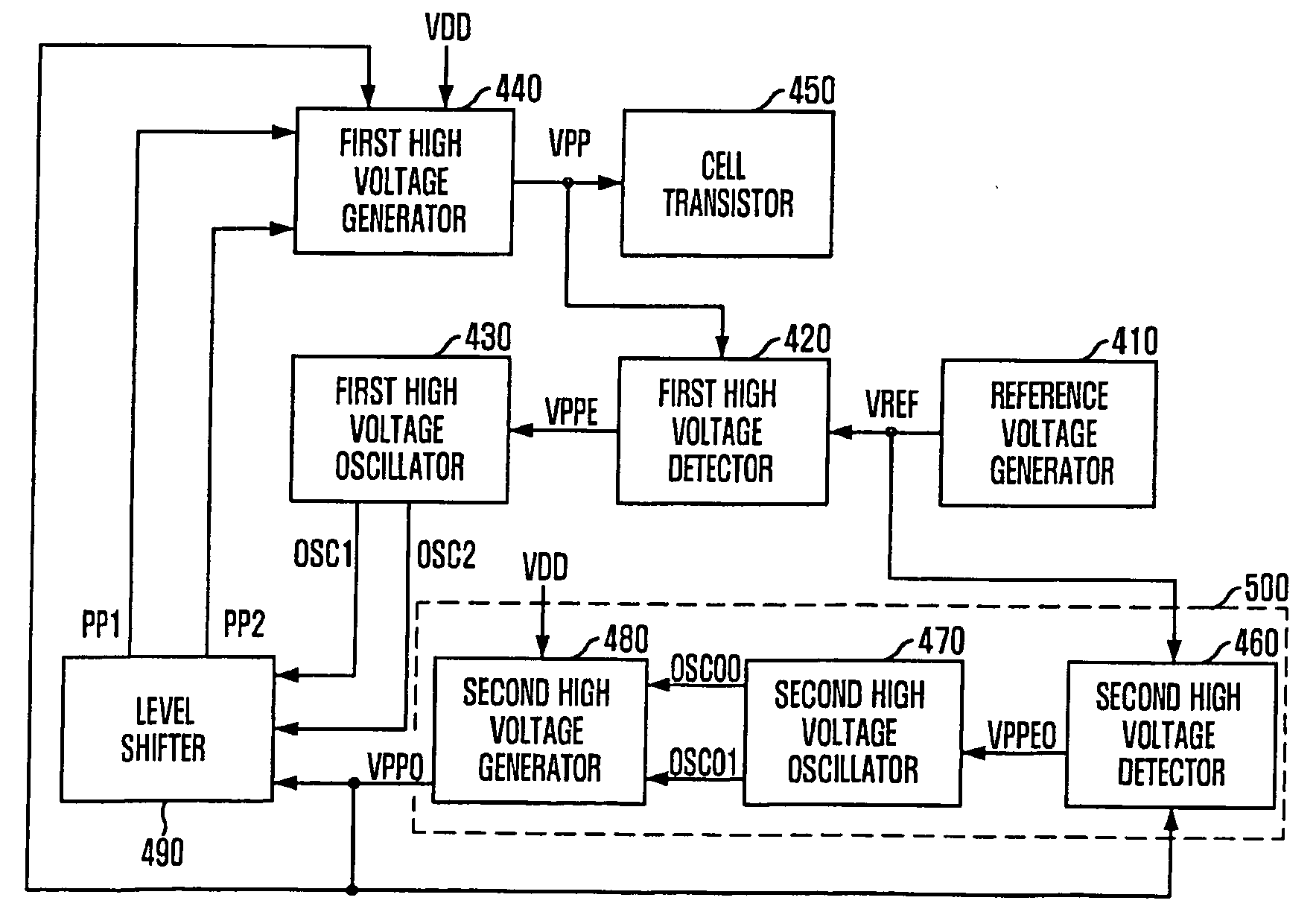
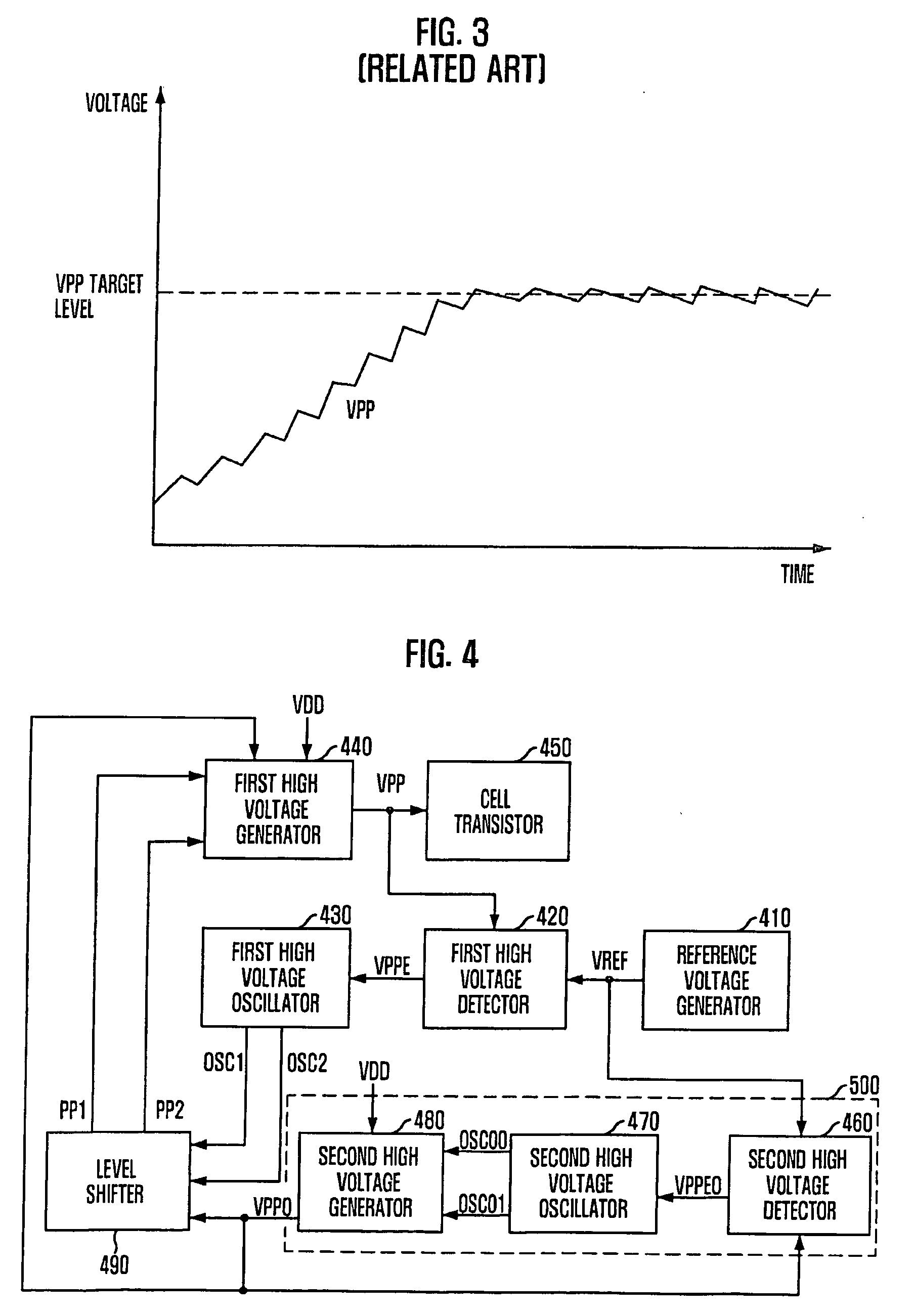
[0033]FIG. 4 is a block diagram illustrating a semiconductor memory device in accordance with an embodiment of the present invention.

[0034]Referring to FIG. 4, the semiconductor memory device includes a reference voltage generator 410, a first high voltage detector 420, a first high voltage oscillator 430, a first high voltage generator 440, a cell transistor 450, a level shifter 490, and a source voltage generator 500. The source voltage generator 500 includes a second high voltage detector 460, a second high voltage oscillator 470, and a second high voltage generator 480. Although the cell transistor 450 is described herein as one example, the high voltage may also be used in various internal components of the semiconductor memory device because internal voltages having various levels are needed f...


PUM


Abstract

A semiconductor memory device that includes a first high voltage oscillator configured to generate a first control pulse in response to a first enable signal, a level shifter configured to generate a high voltage control pulse by boosting a level of the first control pulse using a source high voltage, and a first high voltage generator configured to generate a high voltage by boosting an external power supply voltage in response to the high voltage control pulse.

Description

CROSS-REFERENCE TO RELATED APPLICATIONS[0001]This application claims priority of Korean patent application number 10-2007-0087609, filed on Aug. 30, 2007, which is incorporated by reference in its entirety.BACKGROUND OF THE INVENTION[0002]The subject matter relates to an internal voltage generating circuit of a semiconductor memory device, and more particularly, to a high-voltage generating circuit for boosting a supply voltage to generate a high voltage used in a semiconductor device.[0003]In a system with a variety of semiconductor devices, a semiconductor memory device serves as a data storage. The semiconductor memory device outputs data corresponding to addresses received from a data processor, e.g., a central processing unit (CPU), or stores data received from the data processor into memory cells selected by addresses received from a data processor.[0004]As the integration density of semiconductor memory devices has increased, circuits are designed based on a sub-micron design...

Claims


Application Information

Patent Timeline
Patent Type & Authority Applications(United States)
IPC IPC(8): G11C7/00G11C8/08
CPCG11C11/4074G11C5/145G11C5/14
Inventor KANG, KHIL-OHK
Owner SK HYNIX INC
Why Eureka
Try Eureka