Due to the large number of circuit elements and the required complex layout of the integrated circuits, generally the electrical connection of the individual circuit elements may not be established within the same level on which the circuit elements are manufactured, but requires one or more additional “wiring” layers, also referred to as metallization layers.
Since the fabrication of a plurality of metallization layers entails extremely challenging issues to be solved, such as mechanical, thermal and electrical reliability of many stacked metallization layers that are required, for example, for sophisticated microprocessors, semiconductor manufacturers are increasingly using a metal that allows high current densities and reduced dimensions of the interconnections.
In spite of these advantages, copper also exhibits a number of disadvantages regarding the processing and handling of copper in a semiconductor facility.
For instance, copper may not be efficiently applied onto a substrate in larger amounts by well-established deposition methods, such as chemical vapor deposition (CVD), and also may not be effectively patterned by the usually employed anisotropic etch procedures due to its lack of forming volatile etch byproducts.
A further major drawback of copper is its propensity to readily diffuse in low-k dielectric materials, silicon and silicon dioxide, which is a well-established and approved dielectric material in fabricating integrated circuits.
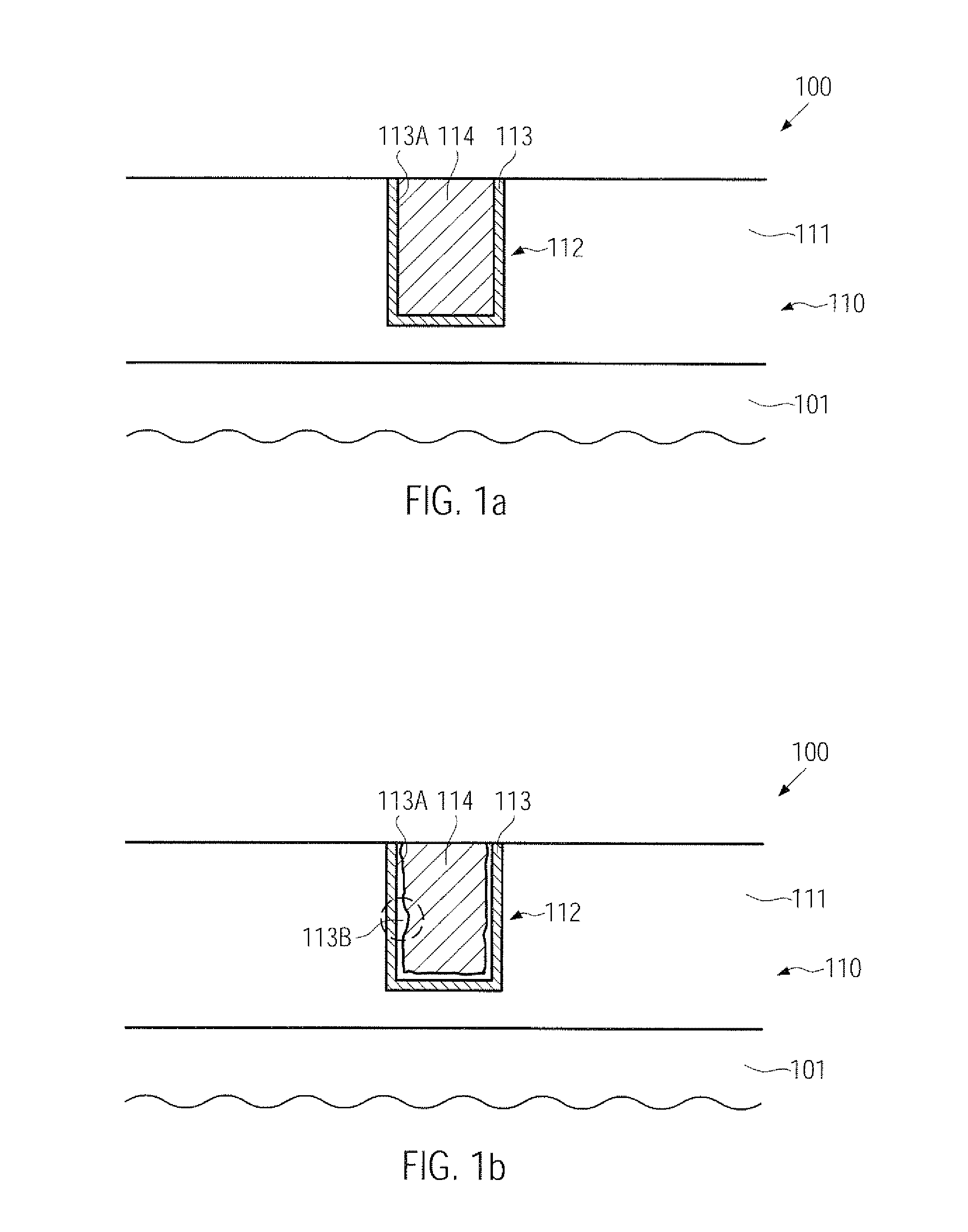
It turns out, however, that a single material may not readily meet the requirements imposed on a desired barrier material.
Tantalum, which effectively blocks copper atoms from diffusing into an adjacent material even when provided in extremely thin layers, however, exhibits only a poor adhesion to a plurality of dielectric materials, such as silicon dioxide based dielectrics, so that a copper interconnection including a tantalum barrier layer may suffer from reduced mechanical stability especially during the chemical mechanical polishing of the metallization layer, which may be employed for removing excess copper and planarizing the surface for the provision of a further metallization layer.
The reduced mechanical stability during the CMP process may, however, entail severe reliability concerns in view of reduced thermal and electrical conductivity of the interconnections.
On the other hand, tantalum nitride exhibits excellent adhesion to silicon dioxide based dielectrics, but has very poor adhesion to copper.
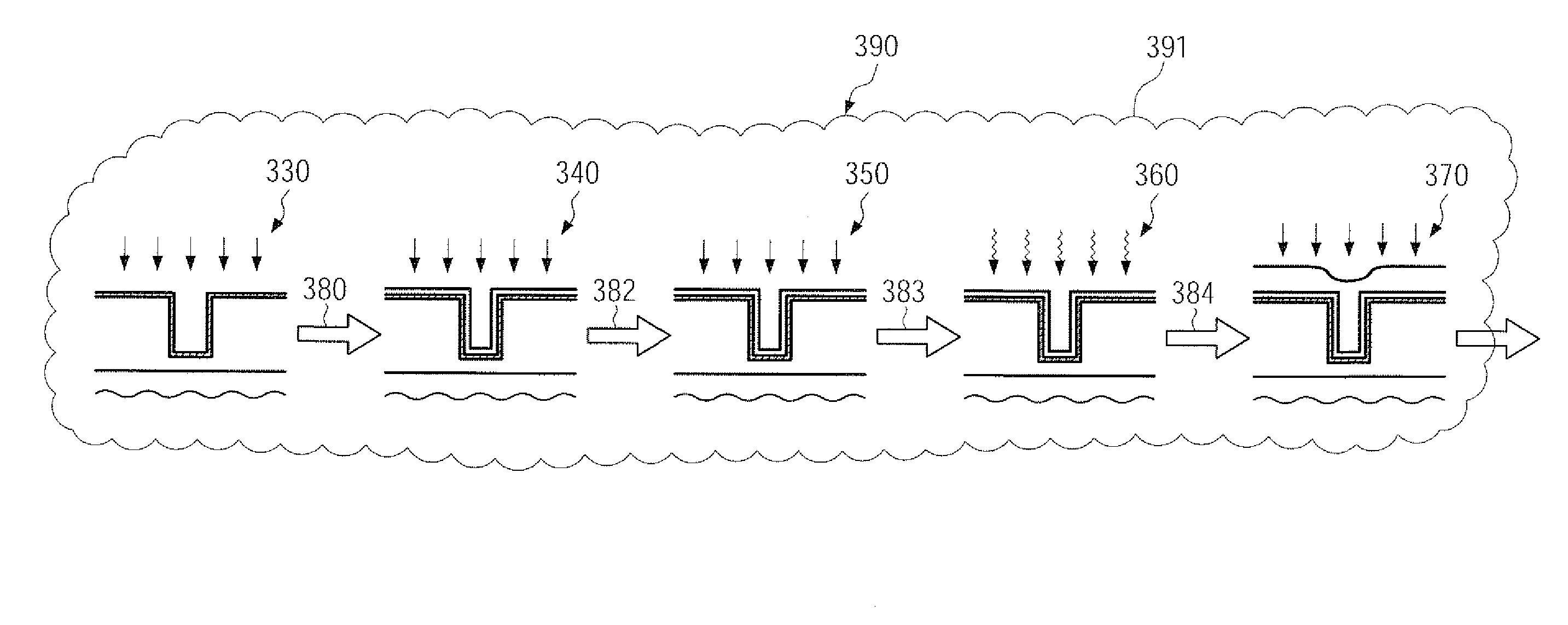
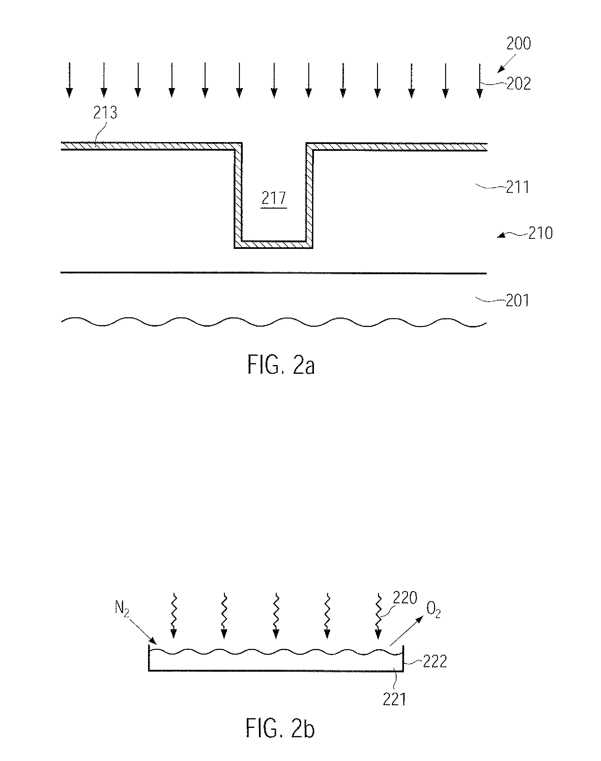
Since the dimensions of the trenches and vias have currently reached a width or a diameter of approximately 0.1 μm and even less with an aspect ratio of the vias of about 5 or more, the deposition of a barrier layer reliably on all surfaces of the vias and trenches and subsequent filling thereof with copper substantially without voids is a most challenging issue in the fabrication of modern integrated circuits.
For dimensions of 0.1 μm and less of vias in future device generations, the sputter deposition of extremely thin metal layers having a high degree of conformity, as required for the barrier layer and the seed layer, may become a limiting factor, since the step coverage characteristics of the above-described advanced sputter tools may not be further enhanced without significant modifications of these tools, which seems to not be a straightforward development.
While the deposition of the barrier layer may be performed on the basis of other highly conformal techniques, such as atomic layer deposition (ALD), which is a well-controllable self-limiting CVD-like process, it appears that the characteristics of the seed layer may be difficult to obtain by these sophisticated techniques, while throughput may also be compromised, thereby making these techniques less attractive for the deposition of the seed material.
Since the deposition of the seed layer may not be performed in a straightforward manner by PVD, and due to the fact that PVD techniques producing extremely thin layers appropriate for barrier layers may result in, when applied to the formation of seed layers, an increased electric resistance, the performance of the final metal region, as well as the initial deposition rate of the subsequent electroplating process, may be negatively affected.
That is, in particular, seed layers formed by advanced CVD techniques may be inferior to commonly used PVD seed layers, due to a significant incorporation of contaminants, thereby resulting in higher electric resistance and weak texture that may, in turn, entail nearly randomly textured metal films.
Although the direct plating is a promising approach, in particular with the prospect of further device scaling, it turns out that performance of the final metal lines and vias, for instance in view of electromigration behavior, crystallinity and thus electrical characteristics, is inferior compared to devices comprising a PVD deposited seed material, thereby making this approach less attractive for usage in mass production of advanced semiconductor devices.
