Method of making a top-emitting OLED device having improved power distribution

Active Publication Date: 2009-03-05
GLOBAL OLED TECH
View PDF10 Cites 17 Cited by
  • Summary
  • Abstract
  • Description
  • Claims
  • Application Information

AI Technical Summary

Benefits of technology

[0018]It is therefore an object of the present invention to provide a method of making a top-emitting LED device having improved power distribution.
[0019]I

Problems solved by technology

However, the current carrying capacity of electrodes formed from these materials is limited, thereby limiting the amount of light that can be emitted.
However, these busses are not useful to provide power to the light-transmissive upper electrode in an OLED device because conventional photolithography techniques destroy the organic layers and a typically thin upper electrode employed in a top-emitting OLED device.
However, this approach has difficulties in that it reduces the light-emitting area of the OLED device and is difficult to manufacture.
In particular, if the auxiliary electrode is formed before the organic elements are deposited, forming a good electrical contact between the upper and auxiliary electrodes is difficult, because the organic materials will be deposited on the auxiliary electrode.
Moreover, undesirable moisture can infiltrate through materials at the corners of the auxiliary electrode and the conformal deposition of an additional upper electrode protection and encapsulation layer is problematic.
If the auxiliary electrode is

Method used


Image

  • Method of making a top-emitting OLED device having improved power distribution
  • Method of making a top-emitting OLED device having improved power distribution
  • Method of making a top-emitting OLED device having improved power distribution

Examples


Embodiment Construction

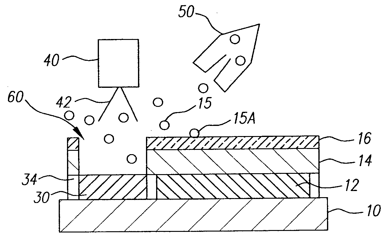
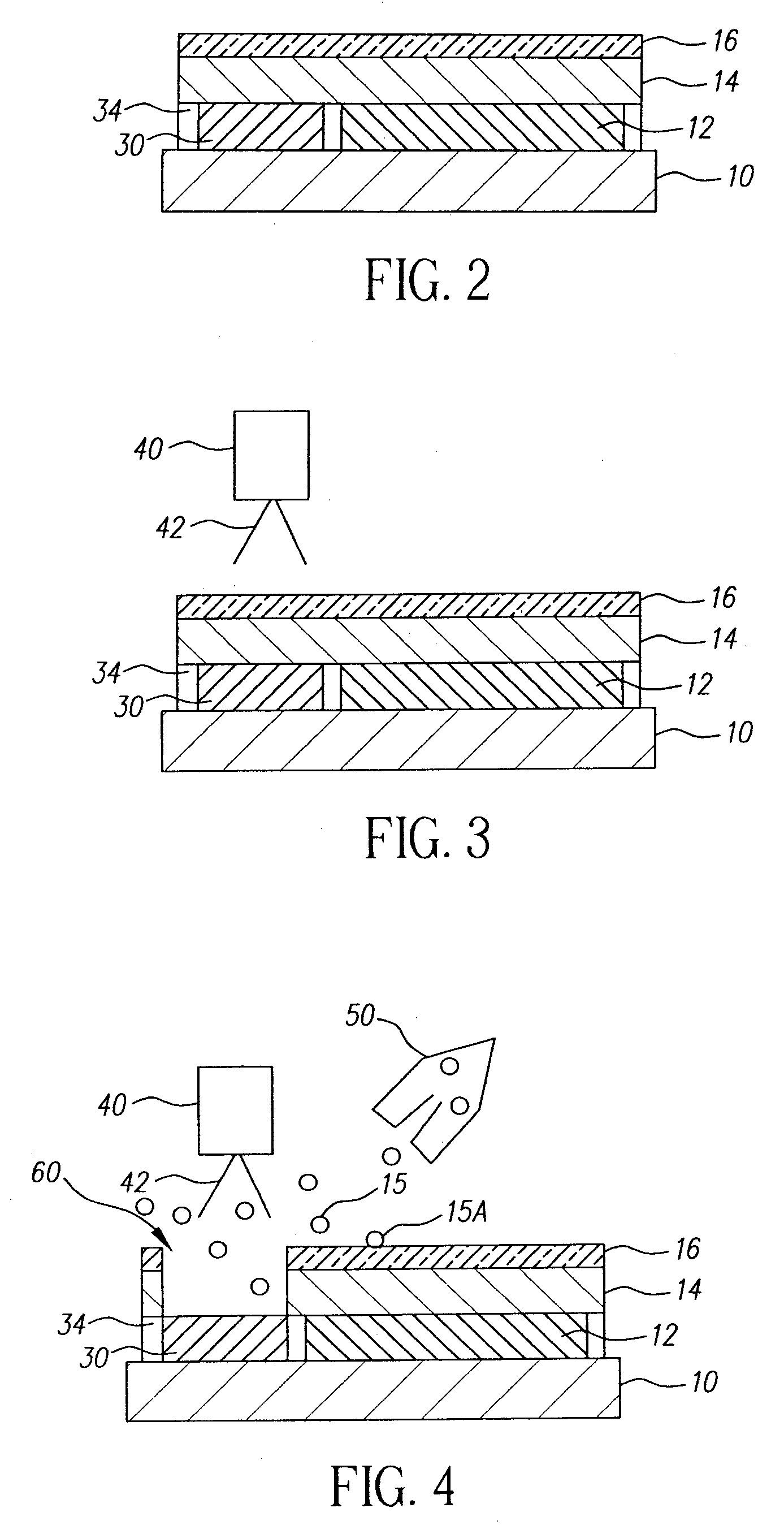
[0034]The present invention is directed to a method of making a top-emitting LED device. In top-emitting LED devices, light is emitted through an upper electrode or top electrode which has to be sufficiently light transmissive, while the lower electrode(s) or bottom electrode(s) can be made of relatively thick and electrically conductive metal compositions which can be optically opaque.

[0035]As used herein, the term “light transmissive” when referring to an upper electrode or top electrode of a top-emitting LED device denotes an optical transmission of 50% or more of light directed perpendicularly at a surface of such electrode. The term “optically opaque” refers to lower electrodes or bottom electrodes, upper electrode busses, bus connectors, and bus connector pads, and denotes an optical transmission of less than 50% of light directed perpendicularly at a surface of such electrically conductive elements.

[0036]The terms “pixel” and “subpixel” are generally used to designate the sma...


PUM


Abstract

A method of making a top-emitting LED device, including providing, over a substrate, a laterally spaced and optically opaque lower electrode and an upper electrode buss that is electrically insulated from the lower electrode; depositing material forming an EL medium structure over the lower electrode and the upper electrode buss; depositing, over the EL medium structure, a first light-transmissive upper electrode that protects the EL medium structure from particulate contamination; and selectively removing most of the EL medium structure over a selective portion of the upper electrode buss.

Description

FIELD OF THE INVENTION[0001]The present invention relates to top-emitting organic light-emitting diode (OLED) devices and, more particularly, to a method of making a top-emitting OLED device having improved power distribution in a light transmissive upper electrode.BACKGROUND OF THE INVENTION[0002]Light-emitting diode (LED) devices, also referred to as electroluminescent (EL) devices, have numerous well-known advantages over other flat-panel display devices currently in the market place. Among these advantages are brightness of light emission, relatively wide viewing angle, and reduced electrical power consumption compared to, for example, liquid crystal displays (LCDs) using backlighting. Such devices may be made with light-emitting layers comprising organic materials or inorganic materials such as quantum dots.[0003]Applications of LED devices include active-matrix image displays, passive-matrix image displays, and area-lighting devices such as, for example, selective desktop ligh...

Claims


Application Information

Patent Timeline
IPC IPC(8): H01J9/02
CPCH01L51/5206H01L2251/5315H01L51/56H01L51/5234H10K50/814H10K50/816H10K50/824H10K50/828H10K50/87H10K2102/3026H10K71/00
Inventor COK, RONALD S.BURBERRY, MITCHELL S.PREUSS, DONALD R.
Owner GLOBAL OLED TECH
Why Eureka
Try Eureka