Semiconductor Device, Manufacturing Method Thereof, and Manufacturing Method of Antenna

a semiconductor and manufacturing method technology, applied in the direction of resonant antennas, instruments, printing, etc., can solve the problems of narrow width of conductive film to be formed, difficult to make fine patterns by just that much, and breakage of conductive film, so as to achieve the effect of improving yield

Inactive Publication Date: 2009-03-12
SEMICON ENERGY LAB CO LTD
View PDF11 Cites 57 Cited by
  • Summary
  • Abstract
  • Description
  • Claims
  • Application Information

AI Technical Summary

Benefits of technology

[0020]When forming a conductive film or the like having a fine form by a screen printing method, by forming a conductive film that is a dummy pattern and then continuing to form a desired conductive film, the conductive film can be formed to be even. As a result, a short circuit between conductive films, a disconnection or the like can be prevented, and yield can be improved.

Problems solved by technology

However, along with downsizing of semiconductor devices, it is necessary to provide a conductive film functioning as an antenna, a conductive film included in a transistor, and the like to be fine, and when a finely-formed conductive film is to be formed by a screen printing method, there is concern for a problem occurring such as a short circuit or a break in the conductive film.
In this manner, when the conductive film with a wider width than that of a form of the opening portion is formed, a problem such as a short circuit occurs by the conductive film coming into contact with an adjacent conductive film 103b.
On the other hand, in a case of widening a distance between opening portions and providing the conductive films in order to prevent the conductive films 103 coming into contact with each other, it becomes difficult to make a fine pattern by just that much.
Further, in a case of making a width of the opening portion narrow and pushing out the paste, a width of a conductive film to be formed becomes narrow, and a problem such as disconnection and decrease in communication range occurs due to breaking and the like.

Method used


Image

  • Semiconductor Device, Manufacturing Method Thereof, and Manufacturing Method of Antenna
  • Semiconductor Device, Manufacturing Method Thereof, and Manufacturing Method of Antenna
  • Semiconductor Device, Manufacturing Method Thereof, and Manufacturing Method of Antenna

Examples


embodiment modes

[0036]Embodiment modes of the present invention will be hereinafter be described with reference to drawings. However, the invention is not limited to the following description, and it is easily understood by those skilled in the art that the modes and details can be changed in various ways without departing from the spirit and scope of the invention. Therefore, the invention is not interpreted limited to the following description of embodiment modes. In the structure of the invention described hereinafter, reference numerals indicating the same things may be used in common in different drawings.

embodiment mode 1

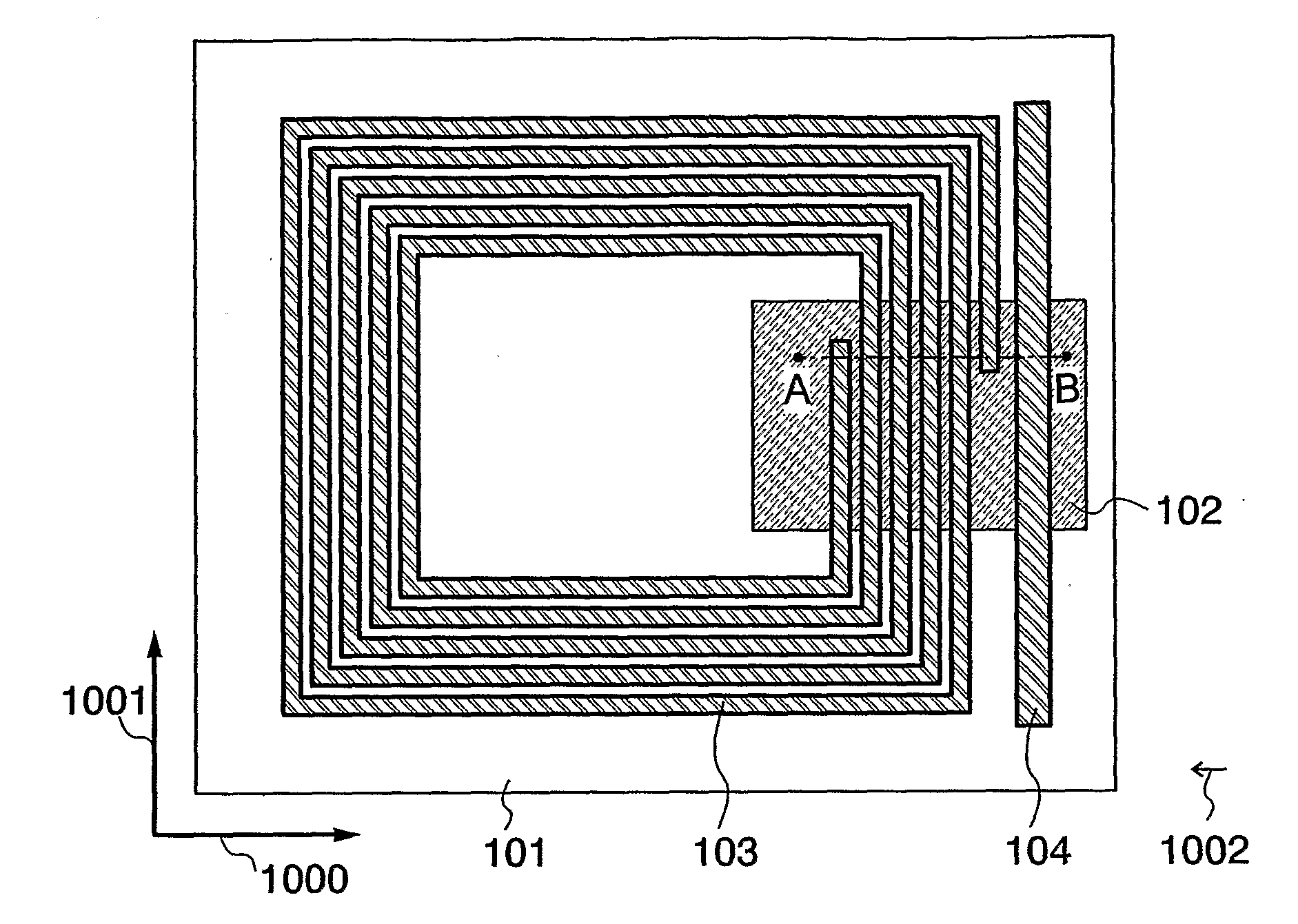
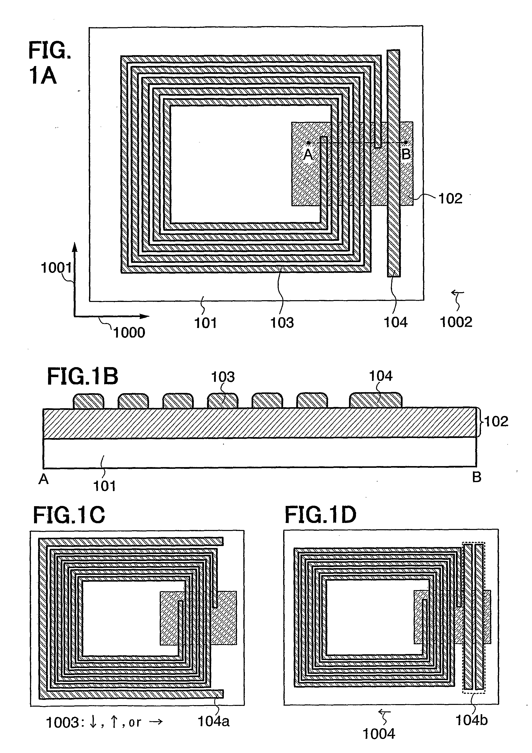
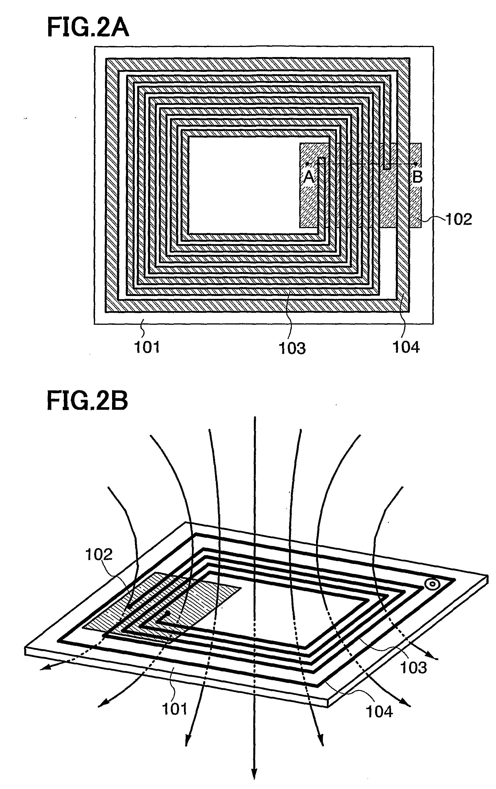
[0037]In this embodiment mode, one example of a semiconductor device of the present invention is described with reference to drawings.

[0038]One example of a manufacturing method of a semiconductor device of the present invention is described hereinafter with reference to drawings.

[0039]First, the element group 102 having a transistor and the like is provided over a substrate 101 (see FIG. 3A).

[0040]As a substrate 101, a glass substrate such as a barium borosilicate glass or an alumino borosilicate glass, a quartz substrate, a ceramic substrate, a metal substrate including stainless steel, or the like can be used. In addition, a semiconductor substrate of Si or the like may be used. Besides those, a substrate formed of a synthetic resin having flexibility such as acrylic or plastic represented by polyethylene terephthalate (PET), a polyethylene naphthalate (PEN), and a polyethersulfone (PES) can be also used. By using a flexible substrate, a bendable semiconductor device can be manuf...

embodiment mode 2

[0066]In this embodiment mode, a structure of a semiconductor device of the present invention different from the structure in the above embodiment mode is described with reference to drawings.

[0067]In a semiconductor device described in this embodiment mode, in the conductive film 103 functioning as an antenna, when the conductive film 103 is provided in a coil form, an average width of the conductive film positioned in an outermost circumference portion (a portion of the conductive film 103 formed on the outermost side) is provided to be wider than an average width of the conductive film formed on an inner side, so as to form the conductive film 105 (see FIGS. 4A and 4B). Note that FIG. 4B shows a schematic view of a cross-section between A and B of FIG. 4A. 4001 is an X axis, and 4002 is a Y axis.

[0068]Also, the width of the entire conductive film 103 positioned in the outermost circumference portion may be provided to be wider than the width of the conductive film formed on the i...


PUM


Abstract

An element group having a transistor is formed over a substrate and a conductive film to be a dummy pattern is formed over the element group by pushing out a paste including conductive particles from a first opening portion, and then a conductive film functioning as an antenna is formed continuously thereafter so as to electrically connect with the transistor, by pushing out a paste including conductive particles from a second opening portion. Therefore, an element group having a transistor, provided over a substrate; a first conductive film functioning as an antenna provided over the element group and is electrically connected to the transistor; a second conductive film to be a dummy pattern provided to be adjacent to the first conductive film and is not electrically connected to the transistor; are included.

Description

TECHNICAL FIELD[0001]The present invention relates to a semiconductor device that is equipped with a conductive film functioning as an antenna and is capable of sending and receiving data without contact, as well as a manufacturing method of the semiconductor device.BACKGROUND ART[0002]In recent years, individual recognition technology has received a lot of attention. For example, there is a technology to be used for production, management, and the like in which information such as a history of the object is clarified by giving an ID (an individual recognition number) to an individual object. Above all, the development of semiconductor devices that can send and receive data without contact has been advanced. As such semiconductor devices, an RFID (Radio Frequency Identification) (also referred to as an ID tag, an IC tag, and IC chip, an RF (Radio Frequency) tag, a wireless tag, an electronic tag, or a wireless chip) and the like are beginning to be introduced into companies, markets...

Claims


Application Information

Patent Timeline
Patent Type & Authority Applications(United States)
IPC IPC(8): G06K19/077B41M1/12H01L21/44
CPCG06K19/07749H01L2924/0002H01L23/5227H01L23/5328H01L27/12H01L27/13H01Q1/38H01Q7/00H01Q9/27H01Q23/00H05K3/1216H01L23/49855H01L27/1292H01L2924/00
Inventor AOKI, TOMOYUKIGOTO, YUUGO
Owner SEMICON ENERGY LAB CO LTD
Why Eureka
Try Eureka