Eureka AIR delivers breakthrough ideas for toughest innovation challenges, trusted by R&D personnel around the world.

Static electricity discharge circuit

Inactive Publication Date: 2009-03-12
SK HYNIX INC
View PDF7 Cites 11 Cited by
  • Summary
  • Abstract
  • Description
  • Claims
  • Application Information

AI Technical Summary

Problems solved by technology

When a high voltage is applied to an integrated circuit due to electrostatic discharge (hereinafter, referred to as ESD), thin insulation layers, channels and so on within the integrated circuit can be damaged by the high voltage and the chip becomes unable to operate normal.

Method used


Image

  • Static electricity discharge circuit
  • Static electricity discharge circuit
  • Static electricity discharge circuit

Examples


Embodiment Construction

.”

BRIEF DESCRIPTION OF THE DRAWINGS

[0027]Features, aspects, and embodiments are described in conjunction with the attached drawings, in which:

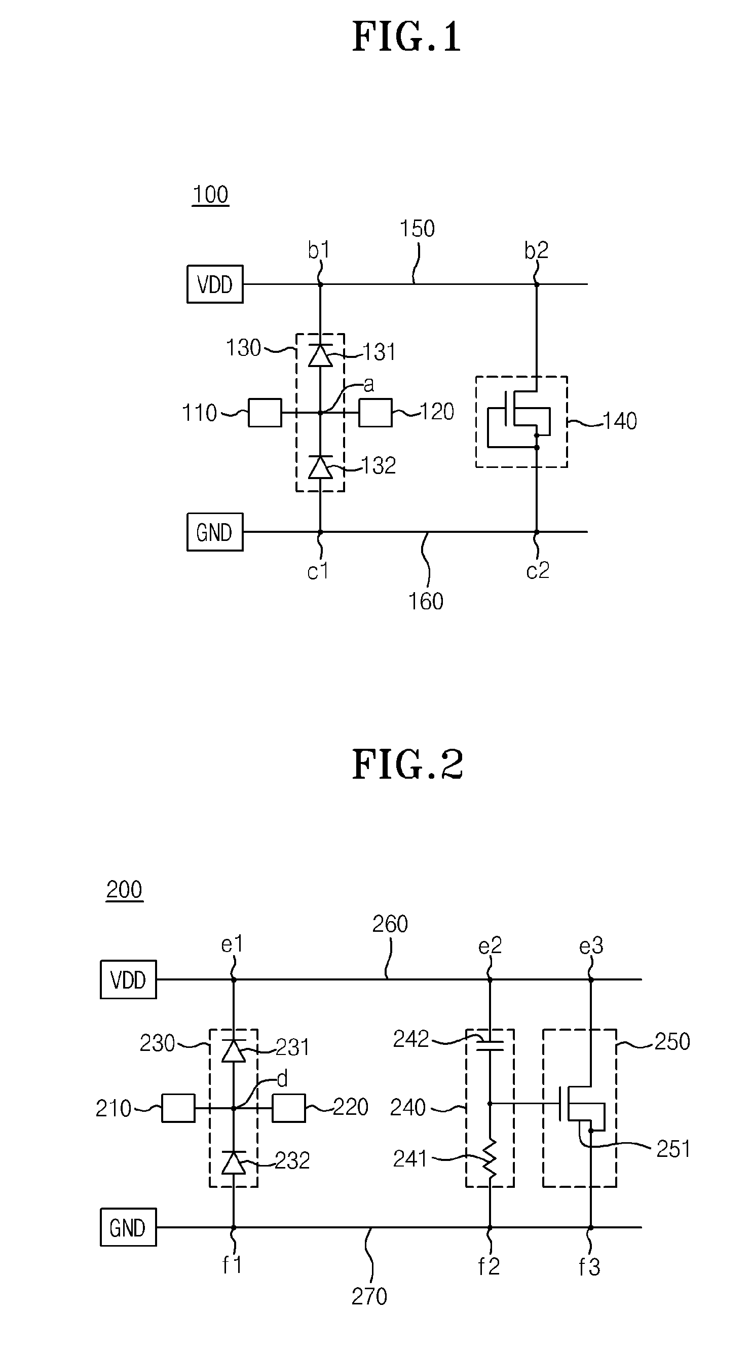
[0028]FIG. 1 is a circuit diagram showing a conventional static electricity discharge circuit.

[0029]FIG. 2 is a circuit diagram showing a conventional RC trigger type static electricity discharge circuit.

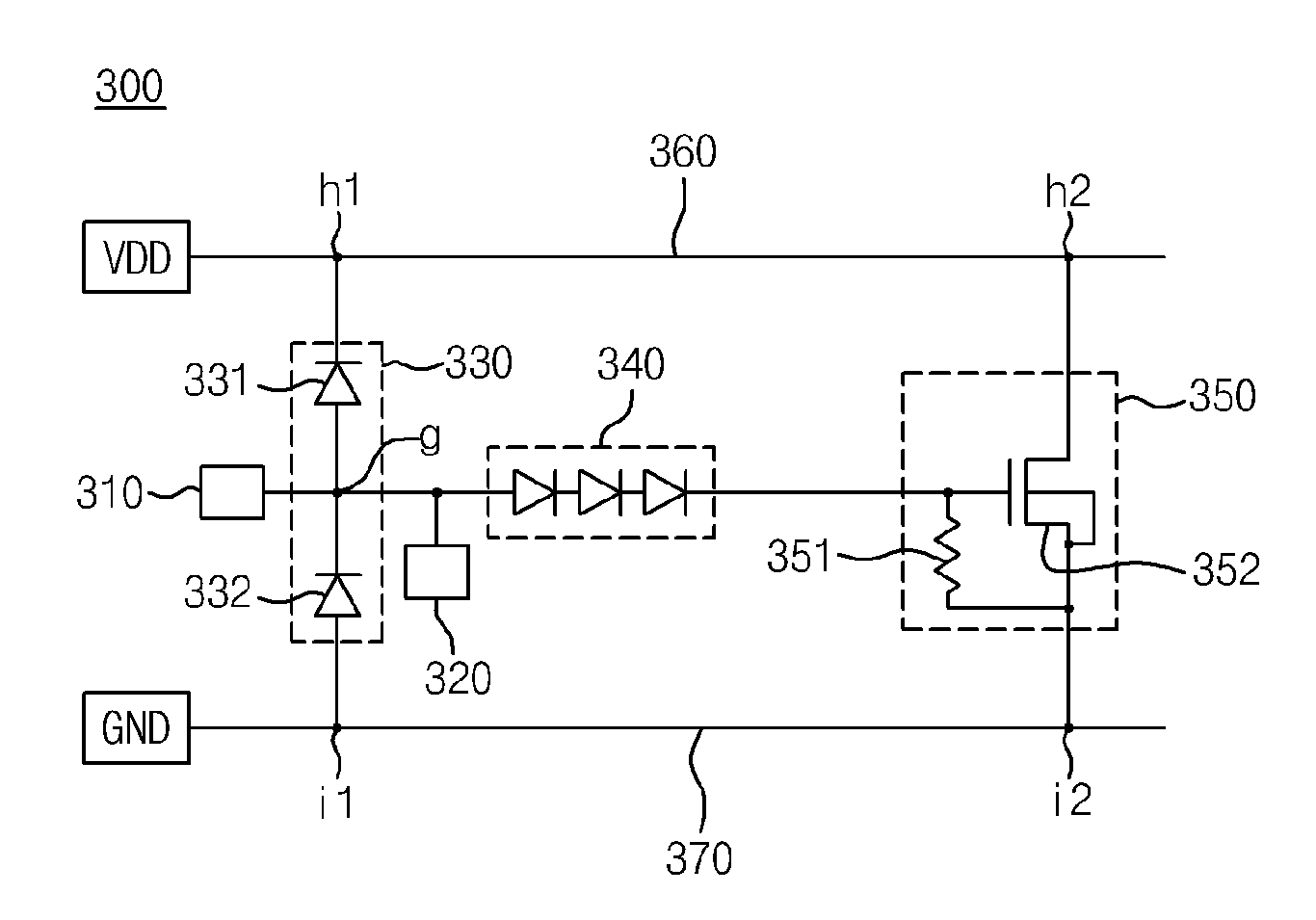
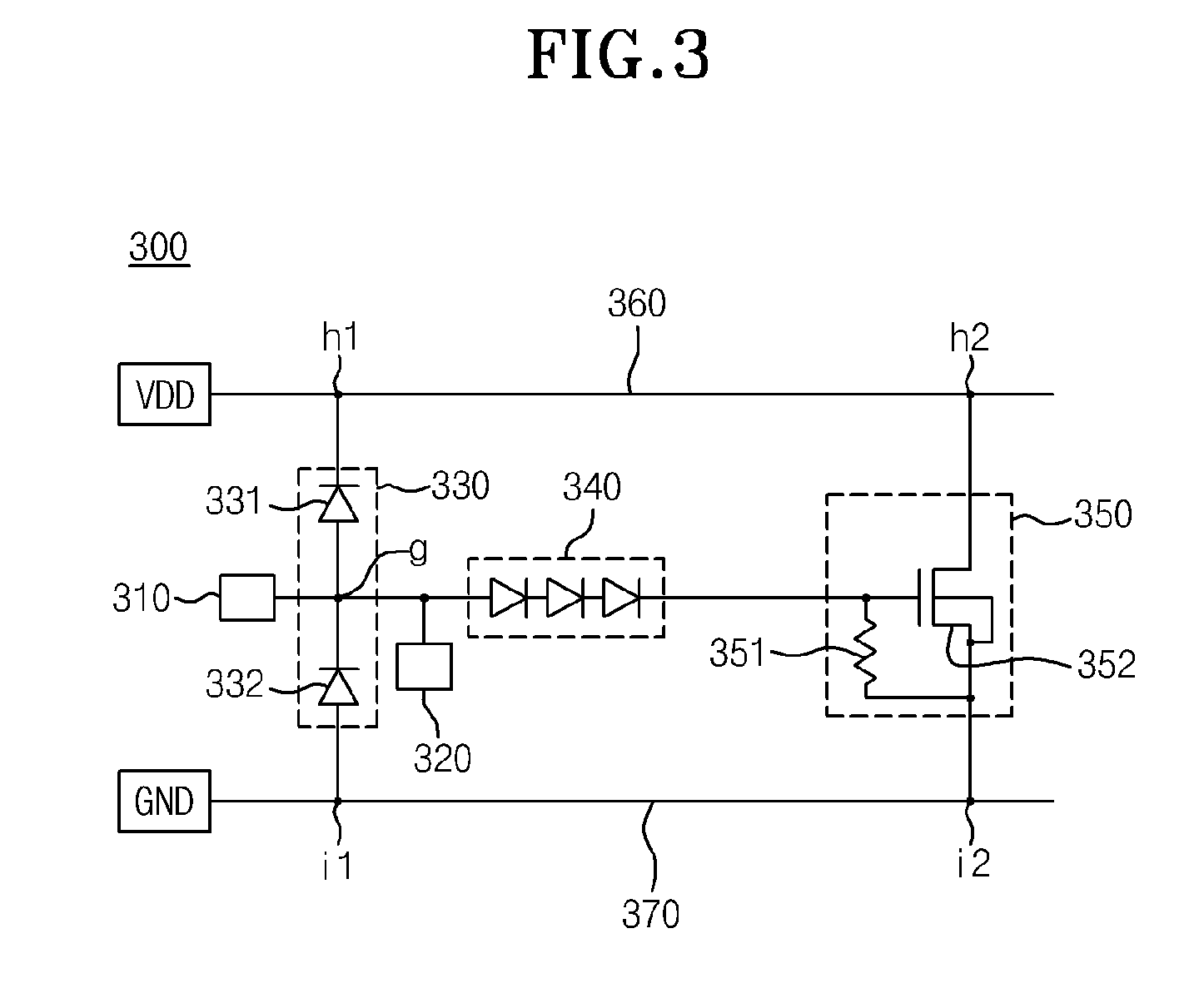
[0030]FIG. 3 is a circuit diagram showing a static electricity discharge circuit according to one embodiment.

[0031]FIG. 4 is a graph comparing trigger voltages for the circuit of FIG. 3 and for the circuits of FIG. 1 and FIG. 2.conventional art.

[0032]FIG. 5 is a graph illustrating current and leakage current in static electricity discharge circuit of FIG. 3.

DETAILED DESCRIPTION

[0033]A static electricity discharge circuit according to the embodiments described herein can operate only when static electricity is applied without influence by an input signal, raise triggering speed, and reduce the circuit area by using a chain diode instead of a ...


PUM


Abstract

A static electricity discharge circuit applied to a highly integrated semiconductor circuit includes a discharge unit connected with the input / output pad by a node and providing, in parallel to the node, a first discharge path connected with a power voltage line and a second discharge path connected with a ground voltage line, an electrostatic detection unit including a diode chain connected to the node and detecting a detection voltage corresponding to static electricity inputted to the node, and a clamp unit switching the discharge path between the power voltage line and the ground voltage line by the detection voltage of the electrostatic detection unit.

Description

CROSS-REFERENCE TO RELATED APPLICATIONS[0001]The present application claims priority under 35 U.S.C. 119(a) to Korean patent application number 10-2007-0091758 filed in the Korean Intellectual Property Office on Sep. 10, 2007, which is incorporated herein by reference in its entirety as if set forth in full.BACKGROUND[0002]1. Technical Field[0003]The embodiments described herein relate to a static electricity discharge circuit, and more precisely, to a static electricity discharge circuit used to prevent defect in a semiconductor device due to a static electricity.[0004]2. Related Art[0005]In general, semiconductor devices are sensitive to the static electricity. When a high voltage is applied to an integrated circuit due to electrostatic discharge (hereinafter, referred to as ESD), thin insulation layers, channels and so on within the integrated circuit can be damaged by the high voltage and the chip becomes unable to operate normal. Therefore, in order to protect the integrated ci...

Claims


Application Information

Patent Timeline
IPC IPC(8): H02H9/04
CPCH02H9/046H01L27/04H01L23/60
Inventor KIM, JANG HOO
Owner SK HYNIX INC
Why Eureka
Eureka Blog
Learn More