Optical sensor circuit

a sensor circuit and optical sensor technology, applied in the field of optical sensor circuits, can solve the problems of affecting the overall uniformity affecting the overall photocurrent conversion characteristics of the optical sensor circuit, and unstable voltage of each node of the feedback loop, so as to achieve fast response properties, wide operating range, and maintain the effect of feedback loop stability

Inactive Publication Date: 2005-06-02
ATLAB INC
View PDF2 Cites 2 Cited by
  • Summary
  • Abstract
  • Description
  • Claims
  • Application Information

AI Technical Summary

Benefits of technology

[0024] It is, therefore, an object of the present invention to provide an optical sensor circuit that continuously keeps a feedback loop stable and provides fast response properties and a wide operating range such that photocurrent conversion is rapidly performed to increase the conversion speed of the optical signal.

Problems solved by technology

In this case, the voltage of an emitter node of the PNP transistor 5 is lowered, so that the PNP transistor 5 turns off and the feedback loop is not maintained nomally, causing each node voltage of the feedback loop to be unstable.
Such an unstable feedback loop also leads to the unstable voltage of the base node of the PNP transistor 5, which degrades the overall photocurrent conversion characteristics of the optical sensor circuit.
Further, while the PNP transistor 5 has an advantage that a current generated by light is amplified, the current amplification factor of the PNP transistor 5 is not uniform among pixels due to a process variation, so that it exerts a bad influence on the overall uniformity of the optical sensor circuit.

Method used


Image

  • Optical sensor circuit
  • Optical sensor circuit
  • Optical sensor circuit

Examples


first embodiment

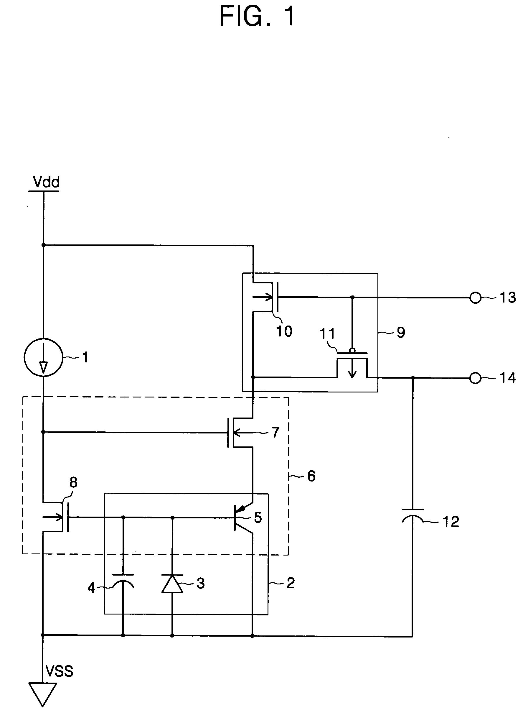
[0035]FIG. 2 is a diagram showing an optical sensor circuit according to the present invention.

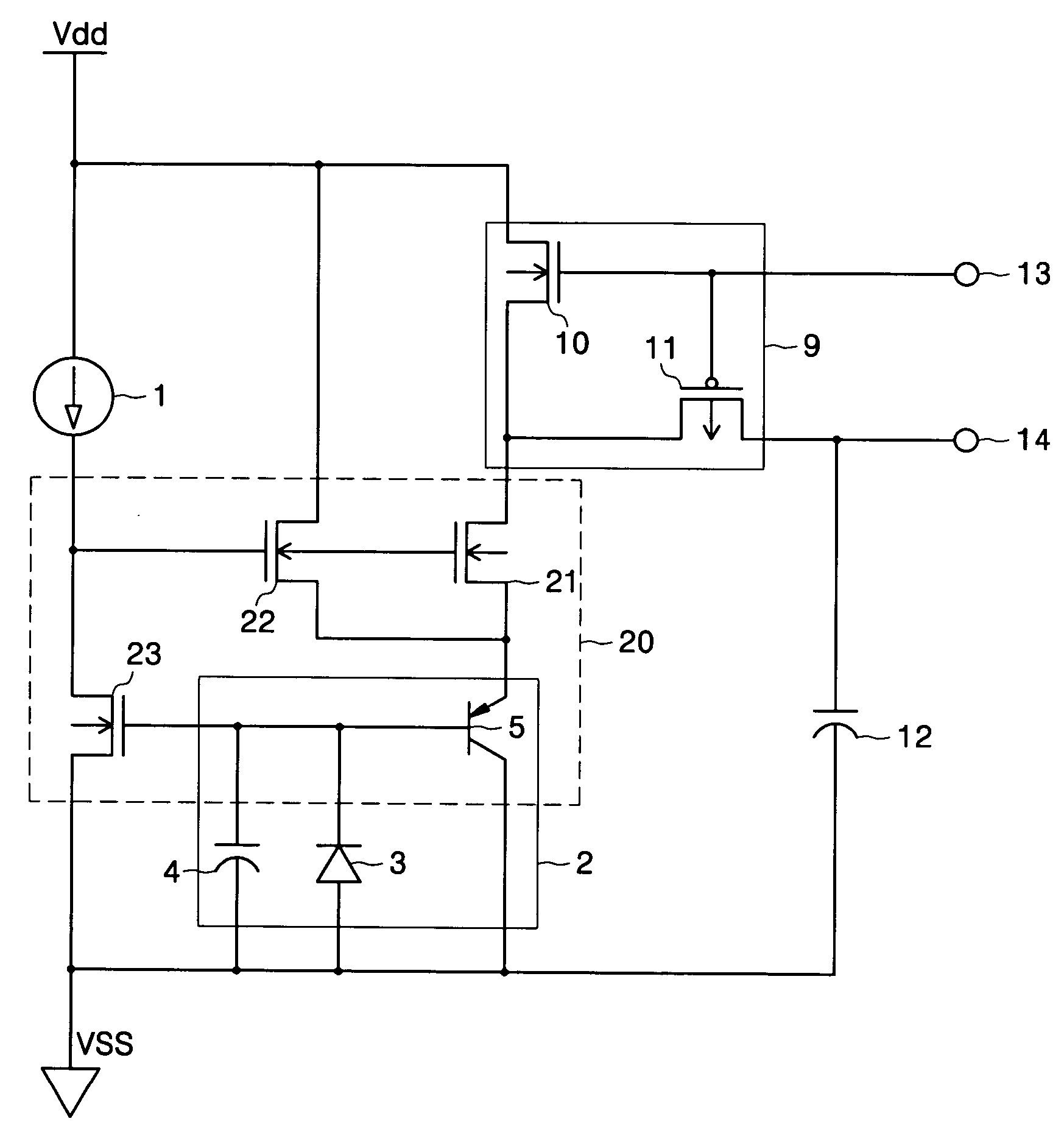
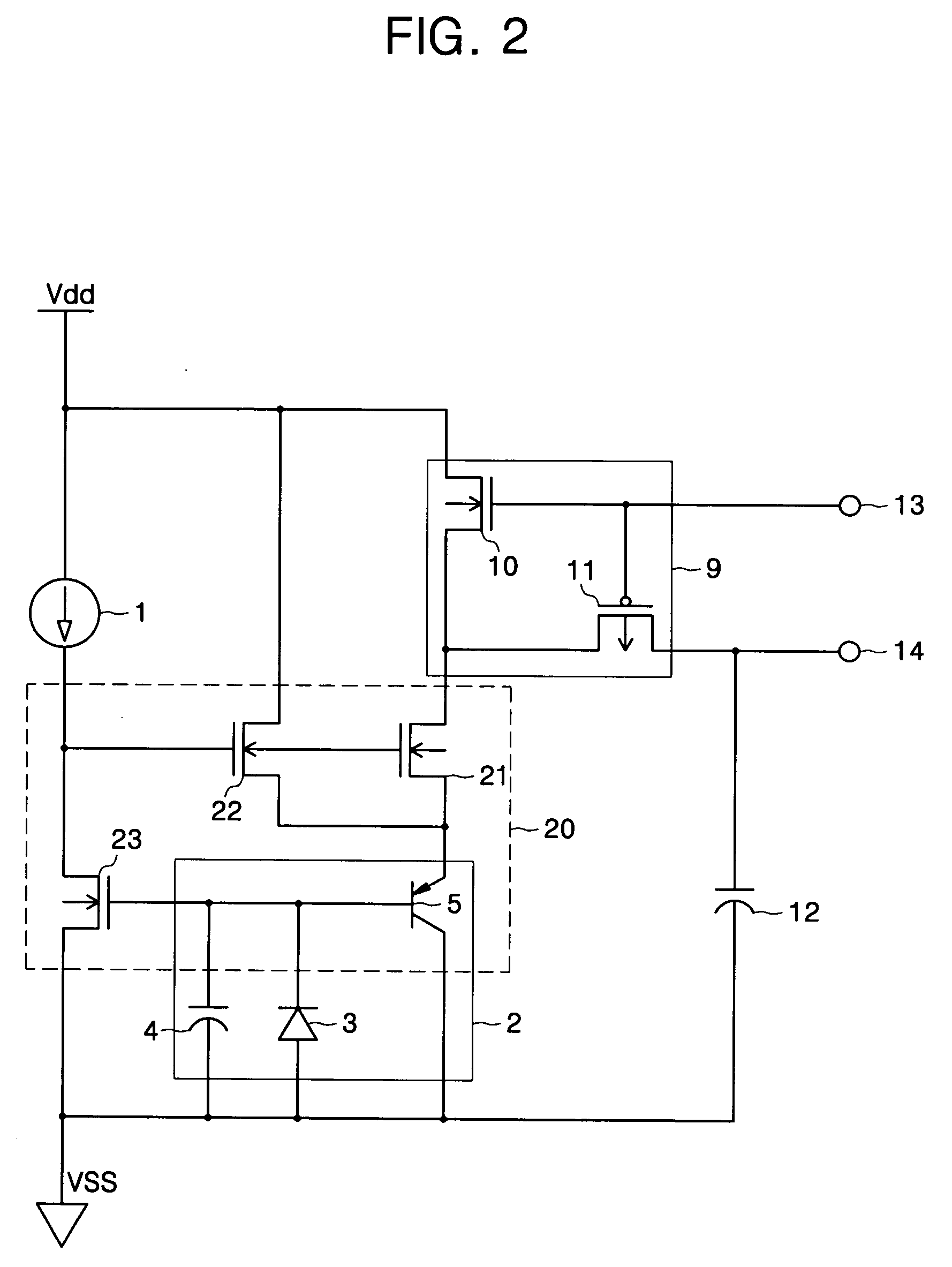
[0036] The optical sensor circuit of FIG. 2 ensures continuous stability of a feedback loop by adding an NMOS transistor 22 to the feedback loop 6 of the optical sensor circuit of FIG. 1. Therefore, like numbers refer to like elements for a circuit that has the same configuration and operation as in FIG. 1 so that the detailed description thereof will be omitted.

[0037] Still referring to FIG. 2, a feedback loop 20 of the optical sensor circuit of the present invention further includes an NMOS transistor 22 where a drain node is connected to a power supply, a gate node is connected to a current source 1, and a source node is connected to a PNP transistor 5.

[0038] In the feedback loop 20, if both an NMOS transistor 10 and a PMOS transistor 11 turn off at the same time during a period that an output control signal transmitted from an output control terminal 13 transitions from Shutter On to...

second embodiment

[0041]FIG. 3 is a diagram showing an optical sensor circuit according to the present invention.

[0042] The optical sensor circuit of FIG. 3 is an example of a circuit that has a wider operating voltage range and improved uniformity of the optical sensor circuit together with the stabilized feedback loop 20 of FIG. 2.

[0043] Like numbers refer to like elements for a circuit that has the same configuration and operation as in FIG. 2 so that the detailed description thereof will be omitted.

[0044] Still referring to FIG. 3, a photocurrent generating unit 30 of the optical sensor circuit of the present invention includes a photodiode 31 that generates a photocurrent in response to the amount of light incident into an optical sensor; and a parasitic capacitor 32 of the photodiode.

[0045] Here, the photocurrent generated in the photodiode 31 is directly delivered to an NMOS transistor 21, and the photocurrent delivered through the NMOS transistor 21 is switched to a feedback loop 20 or a v...

third embodiment

[0048]FIG. 4 is a diagram showing an optical sensor circuit according to the present invention.

[0049] The optical sensor circuit of FIG. 4 is an example of a circuit that has a simpler configuration of the optical sensor circuit together with the stabilized feedback loop 20 of FIG. 2.

[0050] Like numbers refer to like elements for a circuit that has the same configuration and operation as in FIG. 2 so that the detailed description thereof will be omitted.

[0051] Still referring to FIG. 4, a switching unit 44 of the optical sensor circuit of the present invention includes a PMOS transistor 45 that turns on when an output control signal of the switching unit 44 is Shutter On, and turns off when the output control signal is Shutter Off.

[0052] Therefore, a feedback loop 40 is continuously maintained irrespective of operation of the switching unit 44 of the optical sensor circuit, to keep constant a base voltage of a PNP transistor 5.

[0053] The optical sensor circuit of FIG. 4 as descr...


PUM


Abstract

An optical sensor circuit is disclosed. The optical sensor circuit includes: current generating means for generating a photocurrent with an amplitude proportional to the amount of incident light; switching means for switching the photocurrent of the current generating means in response to an output control signal; and circuit stabilizing means for stabilizing operation of the current generating means through an independent current feedback irrespective of operation of the switching means. Therefore, a feedback loop is not affected by the output control signal of an output control unit in order to be stably maintained, so that reliability may be enhanced. Further, by forming the optical sensor circuit with only transistors to be less affected by the process variation, uniformity of the optical sensor circuit may be improved and a wide range of operating voltage may also be provided to increase the signal conversion performance of the optical sensor circuit. Further, the optical sensor circuit may have faster response properties by providing the feedback loop having the high gain.

Description

CROSS-REFERENCE TO RELATED APPLICATION [0001] This application claims the benefit of Korean Patent Application No. 2003-73199, filed Oct. 24, 2003, the disclosure of which is hereby incorporated herein by reference in its entirety. BACKGROUND OF THE INVENTION [0002] 1. Field of the Invention [0003] The present invention relates to an optical sensor circuit and, more particularly, to an optical sensor circuit that converts a light signal into an electrical signal. [0004] 2. Description of the Related Art [0005] A circuit presented in U.S. Pat. No. 6,104,020 is illustrated in FIG. 1 as the prior art. [0006] Referring to FIG. 1, the conventional optical sensor circuit includes a current source 1 that applies a driving current of an optical sensor; a photocurrent generating unit that generates and amplifies a photocurrent in response to the amount of light incident into the optical sensor; a feedback loop that stabilizes an operating voltage of the photocurrent generating unit 2; a volt...

Claims


Application Information

Patent Timeline
Patent Type & Authority Applications(United States)
IPC IPC(8): G01D5/26H01J40/14G01J1/44H01L27/00
CPCH03F3/082H01L31/02019G01J1/44
Inventor JUNG, DEOK-YOUNG
Owner ATLAB INC
Why Eureka
Try Eureka