Method for manufacturing a printed-wiring board having a resistive element

a technology of resistive elements and printed wires, which is applied in the field of manufacturing a printed wire board with a resistive element, can solve the problems of poor resistance value accuracy of resistor patterns formed by screen printing and uniform film thickness, and the range of obtained resistance values is narrow, and achieves low cost, high resistance value accuracy, and high yield

Inactive Publication Date: 2009-03-19
NIPPON MEKTRON LTD
View PDF1 Cites 2 Cited by
  • Summary
  • Abstract
  • Description
  • Claims
  • Application Information

AI Technical Summary

Benefits of technology

[0031]The present invention adjusts a resistance value by performing required trimming for a resistive element which has previously completed resistance changes by applying a lamination history and therefore a changing amount of resistance value after trimming is very small, thus a resistor with high resistance value accuracy can be manufactured with high yield at low cost. Accordingly, a printed-wiring board with built-in resistive element requiring high accuracy, such as a terminal resistor of a transmission line or EMI filter resistor, can be manufactured at low cost and high stability.

Problems solved by technology

The above-described thin-film method can achieve high resistor pattern accuracy; however, the range of an obtained resistance value is narrow because of a thin film.
On the other hand, a resistive paste method provides wide variety of resistance values; however, it is inferior in accuracy of a resistor pattern formed by screen printing and uniformity of film thickness.
It has been known that the resistors formed by the resistive paste method suffer from the resistance value changes, when undergoing laminating press in order to incorporate them in a printed-wiring board.
A variation in the resistance value varies depending upon laminating conditions, type of laminating adhesive agent or film thickness and size of a resistive paste and therefore is difficult to previously estimate the variation of the resistance value due to laminating press before trimming and obtain a desired resistance value after lamination.
However, the method cannot suppress a variation in a resistance value due to lamination.
However, an adjustment method cannot be determined until a resistance value has been measured, which causes a troublesome process.
However, simply filling the hole with paste cannot create a highly accurate resistance value and therefore there occurs such a structure that resistance value adjustment cannot be made even by laser trimming.
However, to heat the resistor, the whole area of the resistor must be scanned with weak laser beams and therefore it takes much time.
This method cannot complete variations in resistance value.
However, the method cannot restrain variations in resistance value due to laminating.
However, a conventional built-in resistive element formed by resistive paste cannot accommodate resistance changes before and after lamination and therefore it is difficult to perform high-yield manufacture with accuracy of ±1 or less, in a built-in state.

Method used


Image

  • Method for manufacturing a printed-wiring board having a resistive element
  • Method for manufacturing a printed-wiring board having a resistive element
  • Method for manufacturing a printed-wiring board having a resistive element

Examples


first embodiment

(First Embodiment)

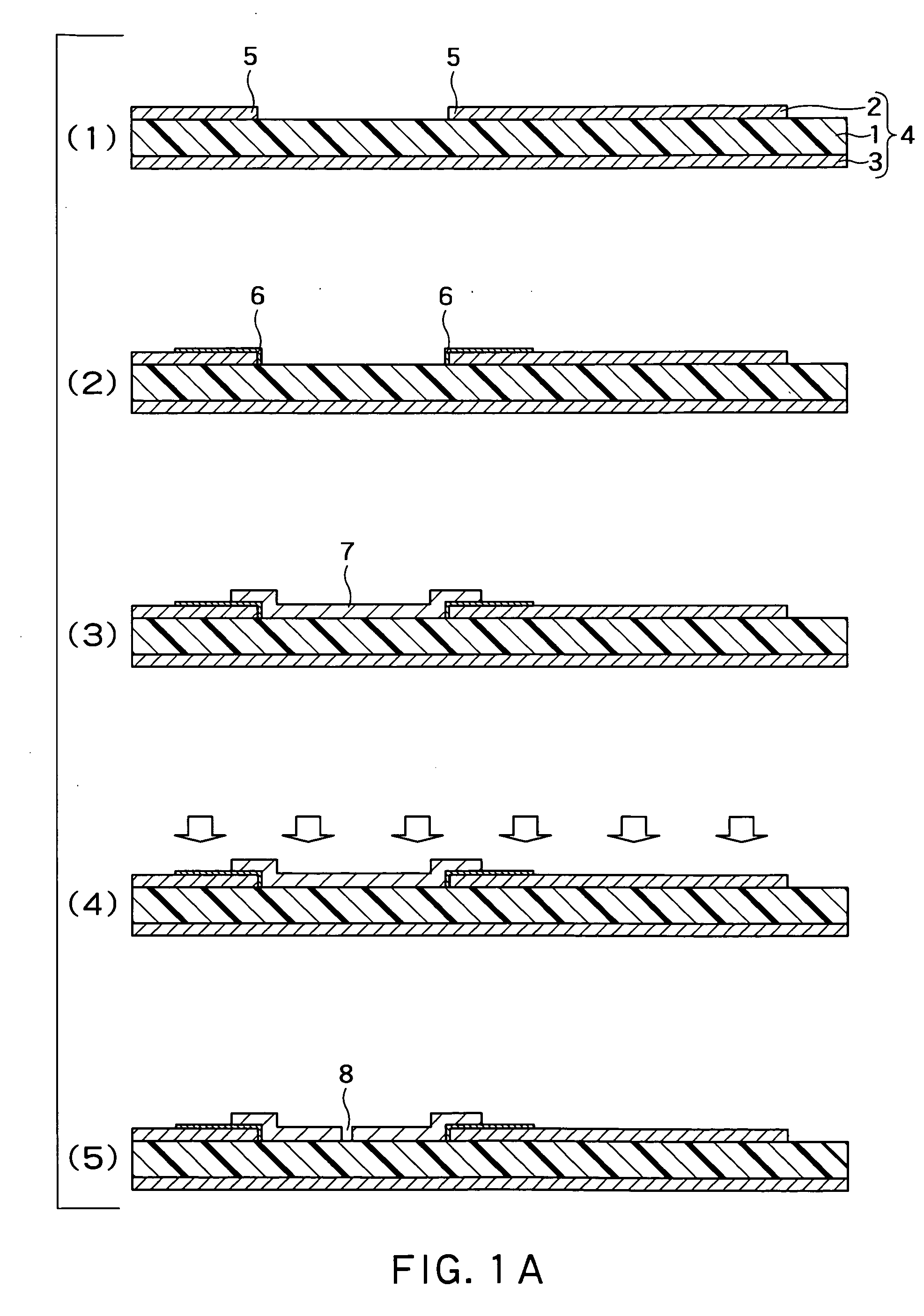
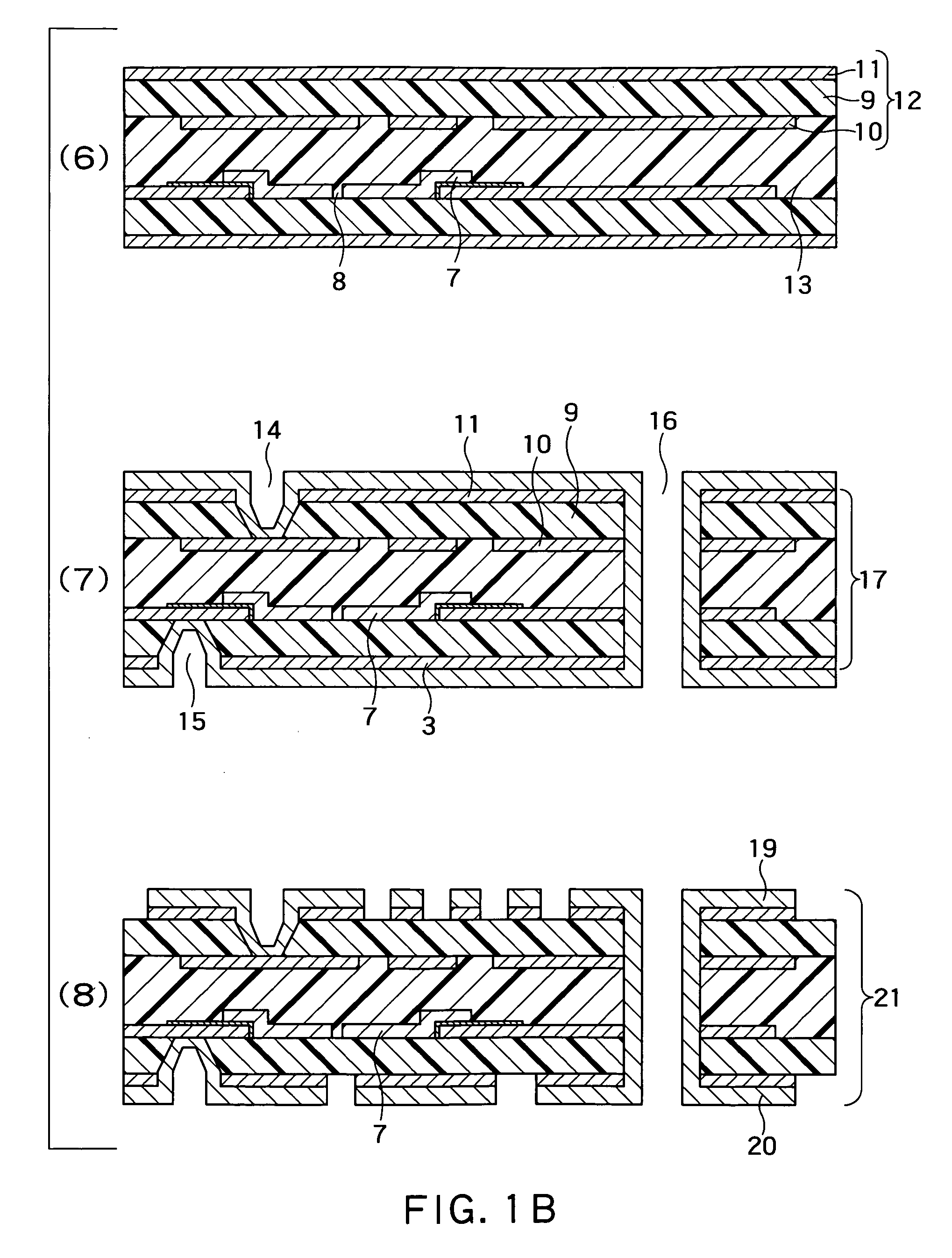
[0036]FIGS. 1A and 1B are a sectional process view illustrating a method for manufacturing a printed-wiring board with built-in resistive element according to one embodiment of the present invention.

[0037]First, as illustrated in FIG. 1A(1), there is prepared a double-sided copper-clad laminate 4 as an organic resin printed-wiring board having a first metal foil 2 such as copper foil and a second metal foil 3 on both faces of an insulating base material 1 such as polyimide as an organic resin insulating layer. At a required position of the first metal foil 2, an electrode 5 for resistor formation is provided, using an etching process by usual photo fabrication and concurrently a circuit is formed.

[0038]For the insulating base material 1, 25μm thick polyimide was used and, for metal foils 2, 3, 12μm thick electrolytic copper foil was used. The resistance value is determined according to width and film thickness of resistive paste, electrode-to-electrode distance and...


PUM

PropertyMeasurementUnit
temperatureaaaaaaaaaa
thickaaaaaaaaaa
thickaaaaaaaaaa

Abstract

A method for manufacturing a printed-wiring board having an organic resin insulating layer and a metal wiring layer and having a film-like resistive element formed on the metal wiring layer thereof, the method including: disposing a metal wiring layer on one surface of one organic resin insulating layer 1 to form an organic resin printed-wiring board 4; forming a pair of electrodes 5 on the metal wiring layer of the organic resin printed-wiring board; forming a film-like resistive element 7 between the electrodes; applying a temperature and a pressure of a laminating press to the side of the metal wiring layer in the wiring board without use of a laminating adhesive agent to change a resistance value of the film-like resistive element; trimming the film-like resistive element for adjusting a resistance value; providing a circuit member 12 having at least one layer of insulating layer; and laminating the circuit member with a laminating adhesive agent 13 in between so as to contact with a layer of the organic resin printer-circuit board having the film-like resistive element formed thereon. Accordingly, the present invention provides a method for manufacturing a printed-wiring board with built-in resistive element formed by resistive paste with high accuracy and high yield at low cost.

Description

CROSS REFERENCE TO RELATED APPLICATIONS[0001]This application is based upon and claims the benefit of priority from the prior Japanese Patent Application No. 2007-241978, filed on Sep. 19, 2007, the entire contents of which are incorporated herein by reference.BACKGROUND OF THE INVENTION[0002]1. Field of the Invention[0003]The present invention relates to a method for manufacturing a printed-wiring board and, in particular, to a method for manufacturing a printed-wiring board having a resistive element therein.[0004]2. Related Art[0005]In recent years, with miniaturization and high functionality of an electronic device, the mounting density of components has remarkably increased. Accordingly, a printed-wiring board having built-in components with increased mounting density has been studied, in which passive components are formed on an inner surface of the printed-wiring board, which will replace a conventional method: soldering passive components such as resistors and capacitors on ...

Claims


Application Information

Patent Timeline
Patent Type & Authority Applications(United States)
IPC IPC(8): B32B37/02
CPCH05K1/167H05K3/4611H05K2203/0278Y10T156/1052H05K2203/171Y10T156/1062H05K2203/1453
Inventor MIYAMOTO, GARO
Owner NIPPON MEKTRON LTD
Why Eureka
Try Eureka