Check patentability & draft patents in minutes with Patsnap Eureka AI!

Image sensor and method for manufacturing the same

a technology of image sensor and manufacturing method, which is applied in the field of image sensor, can solve the problems of difficult manufacturing such a multi-layer laminated image pickup device, image blurring, and inability to use flexible substrates made of plasti

Active Publication Date: 2009-03-19
SAMSUNG DISPLAY CO LTD
View PDF3 Cites 76 Cited by
  • Summary
  • Abstract
  • Description
  • Claims
  • Application Information

AI Technical Summary

Problems solved by technology

However, a gap equivalent to the thickness of the substrate (intermediate substrate) intervening between the light-receiving pixels is formed, resulting in a problem that images are apt to be blurred.
However, it is difficult to manufacture such a multi-layer laminated image pickup device, since the electrode of each laminated light-receiving pixel is required to be connected to the transmission and read-out circuit formed on the substrate.
Furthermore, since the transmission and read-out circuit formed on the substrate is made of a silicon semiconductor that requires a high temperature process, a flexible substrate made of plastic cannot be used.

Method used


Image

  • Image sensor and method for manufacturing the same
  • Image sensor and method for manufacturing the same
  • Image sensor and method for manufacturing the same

Examples


Embodiment Construction

[0016]Hereinafter, embodiments of the invention will be explained with reference to the drawings.

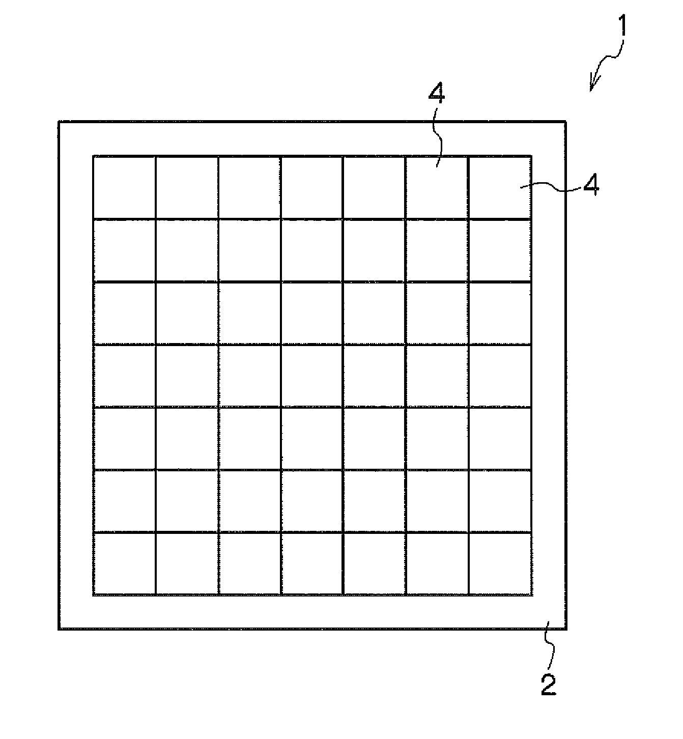
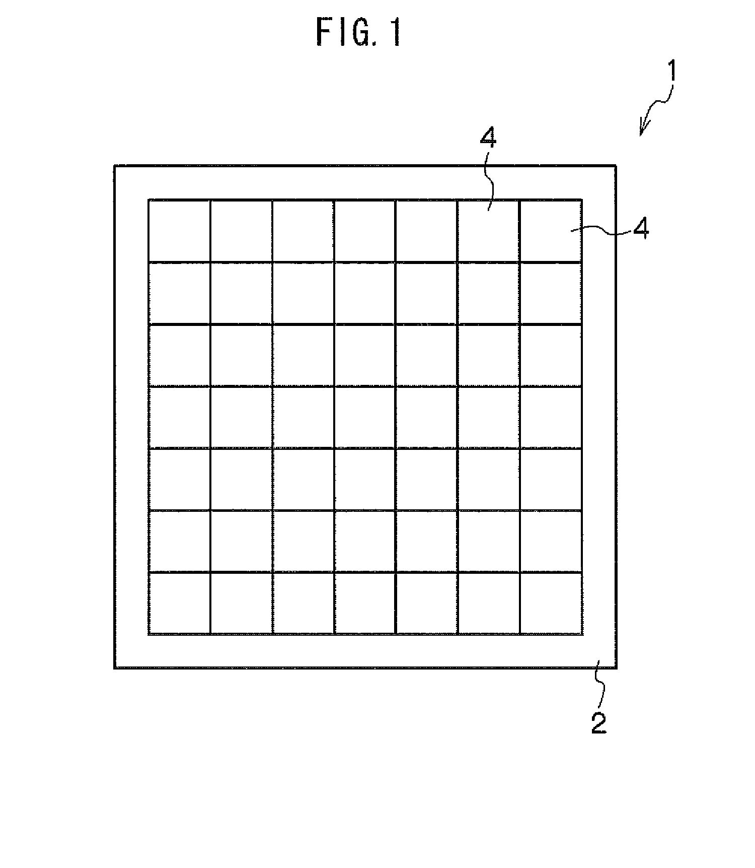
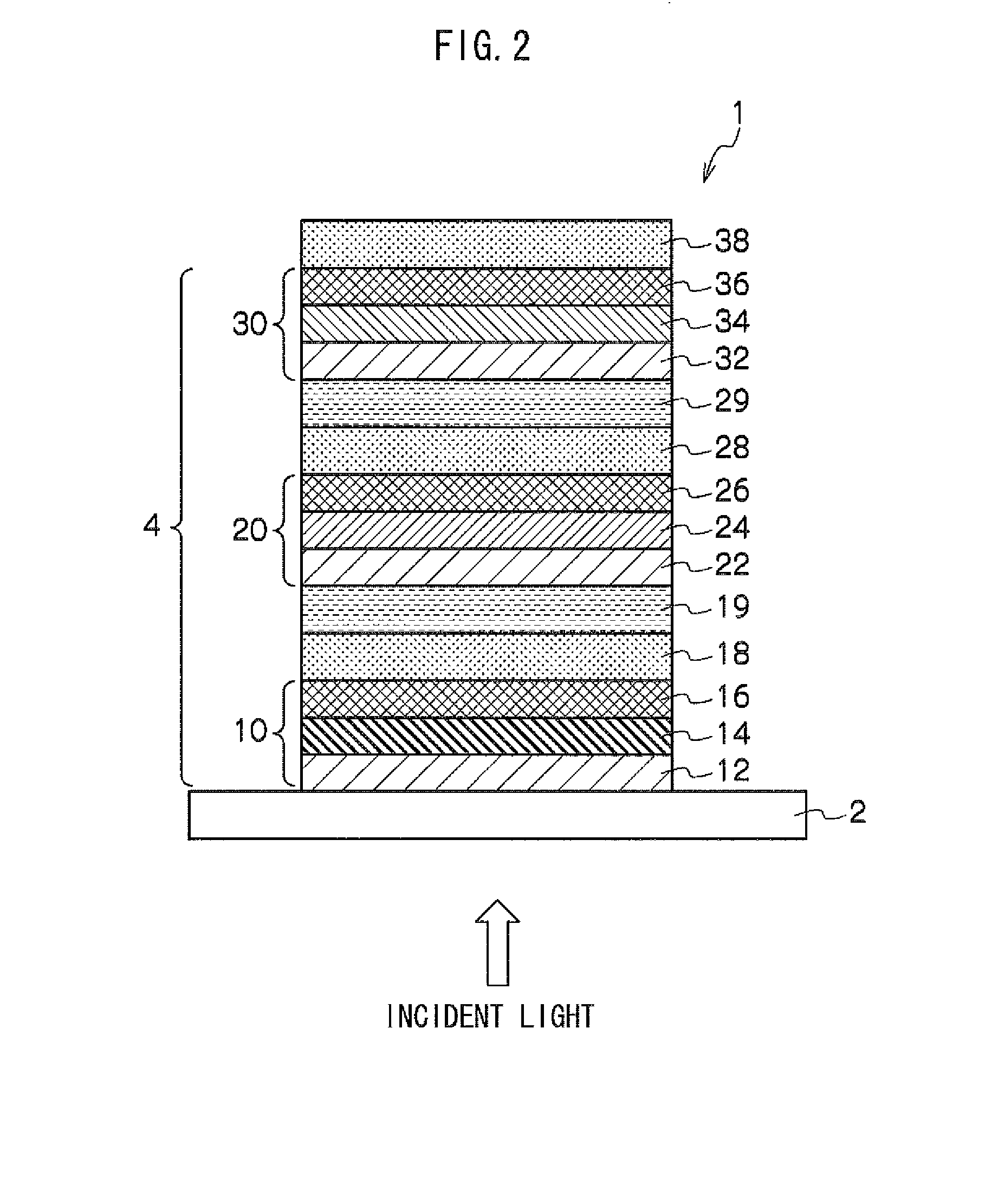
[0017]FIG. 1 is a schematic plan view showing an example of the array of primary light-receiving pixels 4 in a surface direction of a substrate 2 of an image sensor 1 according to one embodiment. FIG. 2 is a schematic sectional view showing an example of the layer configuration of secondary light-receiving pixels 10, 20 and 30 constituting the primary light-receiving pixels 4.

[0018]As shown in FIG. 2, the image sensor 1 according to the embodiment is formed by laminating sequentially three kinds of light-receiving pixels (secondary light-receiving pixels) 10, 20, and 30 which are selectively sensitive to lights in different wavelength ranges (B, G and R), respectively, on one surface of a substrate 2 in the thickness direction. Further, scaling insulation layers 18 and 28, and planarization layers 19 and 29 intervene between secondary light-receiving pixels which are adjacent to each oth...


PUM


Abstract

An image sensor 1 has a substrate 2 and primary light-receiving pixels 4 arrayed in the direction of the surface of the substrate, and the primary light-receiving pixels are formed by laminating plural secondary light-receiving pixels 10, 20 and 30 which sense lights in different wavelength ranges, respectively, via at least sealing insulation layers 18 and 28 between adjacent secondary light-receiving pixels in the thickness direction. Each secondary light-receiving pixel includes a photoelectric conversion portion 14, 24, or 34 for photoelectrically converting the lights and a signal output portion 12, 22 or 32 for outputting signals from a thin film transistor 40 according to charges generated by the photoelectric conversion portion, and the active layer 48 of the thin film transistor is formed from an oxide semiconductor or organic semiconductor.

Description

CROSS REFERENCE TO RELATED APPLICATION[0001]This application claims priority under 35 USC 119 from Japanese Patent Application No. 2007-238257, the disclosure of which is incorporated herein by reference.BACKGROUND OF THE INVENTION[0002]1. Field of the Invention[0003]The present invention relates to an image sensor and a method of manufacturing the sensor, in particular, to an image sensor suitable for a contact image sensor, an image acquiring device and the like.[0004]2. Description of the Related Art[0005]As an image sensor, there is a type in which three kinds of light-receiving pixels that selectively receive lights in different wavelength ranges, for example, lights of three primary colors of red (R), green (G) and blue (B), respectively, are arrayed so as to be arranged on a substrate. In such an image sensor formed by arraying light-receiving pixels corresponding to the three primary colors of R, G and B, an image can be picked up in full color. However, the resolution of su...

Claims


Application Information

Patent Timeline
IPC IPC(8): H01L27/00H01L27/146H01L31/02H04N5/335H04N5/369H04N5/374
CPCH01L27/14647
Inventor TADA, HIROSHIHAYASHI, MASAYUKINAKAYAMA, MASAYA
Owner SAMSUNG DISPLAY CO LTD
Features
  • R&D
  • Intellectual Property
  • Life Sciences
  • Materials
  • Tech Scout
  • Unparalleled Data Quality
  • Higher Quality Content
  • 60% Fewer Hallucinations
Learn More