Photocoupler
a photocoupler and photoelectric technology, applied in the field of photocouplers, can solve the problems of narrow operating range of inspection mode and some techniques
- Summary
- Abstract
- Description
- Claims
- Application Information
AI Technical Summary
Benefits of technology
Problems solved by technology
Method used
Image

Examples
first embodiment
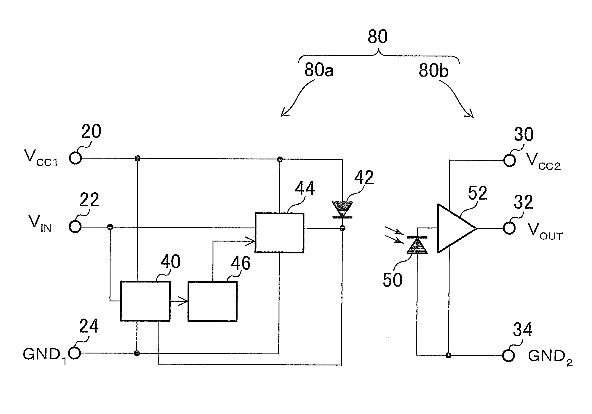
[0020]FIG. 1 is a block diagram for describing a photocoupler according to the invention. The photocoupler 80 includes a light emitting section 80a and a light receiving section 80b. The light emitting section 80a includes a VCC1 terminal 20 to which a power supply voltage (hereinafter VCC1) is applied, a VIN terminal 22 to which an input voltage (hereinafter VIN) is inputted, a ground (hereinafter GND1) terminal 24, a light emitting device 42 made of semiconductor, a clamp circuit 40, a drive circuit 44, and a drive stop circuit 46. Here, GND1 is the ground of the system or device. The light receiving section 80b includes a VCC2 terminal 30 to which a power supply voltage (hereinafter VCC2) is applied, a VOUT terminal 32 from which an output voltage (hereinafter VOUT) is outputted, a ground (hereinafter GND2) terminal 34, a photodiode 50, and a light receiving circuit 52.
[0021]A digital signal inputted to the VIN terminal 22 causes the drive circuit 44 to turn on / off the light emit...
second embodiment
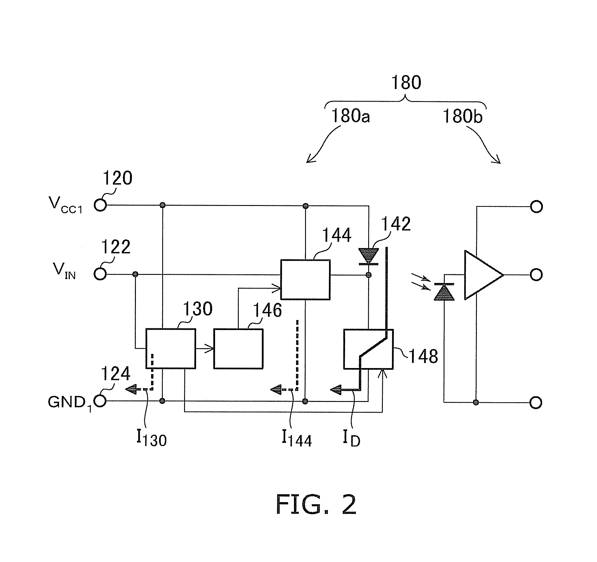
[0033]FIG. 4 is a circuit diagram of the photocoupler according to a Its block diagram can be represented by FIG. 1. In this embodiment, the clamp circuit 40 is set to a potential lower than GND1. For example, in the case of clamping at (GND1 potential −500 mV), the potential VB at point P is set by division with resistors R6 and R7. More specifically, if VF is 700 mV and VB is set to 200 mV, then transistors Q6 and Q7 are turned on at (GND1 potential −500 mV), a current flows therethrough, the voltage across resistor R9 drops, and the output voltage of Q7 decreases.
[0034]Furthermore, the drive stop circuit 46 detects the inspection mode and stops the operation of the drive circuit 44. The collector of Q6 is connected to the cathode of the light emitting device 42, and 16 flows therethrough. If the current flowing through Q7 is sufficiently small, the current I6 flowing through the light emitting device 42 is generally equal to ICL. Thus, the sensitivity and the like of the light e...
third embodiment
[0038]FIG. 5 is a block diagram showing a third embodiment, and FIG. 6 is a circuit diagram thereof. As in this embodiment, it is also often the case that the light emitting device 42 is placed and driven on the GND side.
[0039]In FIG. 6, when VIN is lower than VCC1, the drive circuit 44 detects the operation mode and drives the light emitting device 42. On the other hand, when VIN is higher than VCC1 by VF, transistors Q8 and Q9 are turned on, and a current flows therethrough. The voltage drop across R12 causes the output voltage of Q9 to increase. Thus, the inspection mode is detected, and the operation of the drive circuit 44 is stopped. If the current flowing through Q9 is sufficiently small, the clamp current ICL is generally equal to the collector current I8 flowing through Q8. Thus, the light emitting device 42 is driven, and the analog operating characteristics such as current sensitivity of the light emitting device 42 can be accurately measured.
PUM
 Abstract
Description
Claims
Application Information