Electromagnetic shield formation for integrated circuit die package

a technology of integrated circuits and die packages, applied in the field of integrated circuit shielding, can solve problems such as incompatibility of methods with packaging processes

Inactive Publication Date: 2009-03-19
NORTH STAR INNOVATIONS
View PDF1 Cites 153 Cited by
  • Summary
  • Abstract
  • Description
  • Claims
  • Application Information

AI Technical Summary

Problems solved by technology

However, such methods may not be compatible with packaging processes where post interconnect processing is performed after die encapsulation.

Method used


Image

  • Electromagnetic shield formation for integrated circuit die package
  • Electromagnetic shield formation for integrated circuit die package
  • Electromagnetic shield formation for integrated circuit die package

Examples


Embodiment Construction

[0029]The following sets forth a detailed description of a mode for carrying out the invention. The description is intended to be illustrative of the invention and should not be taken to be limiting.

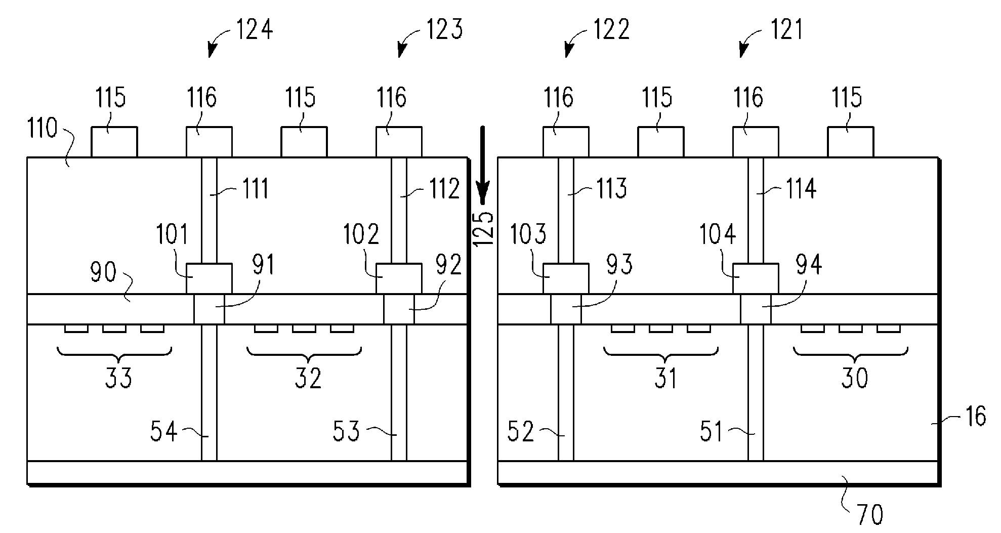
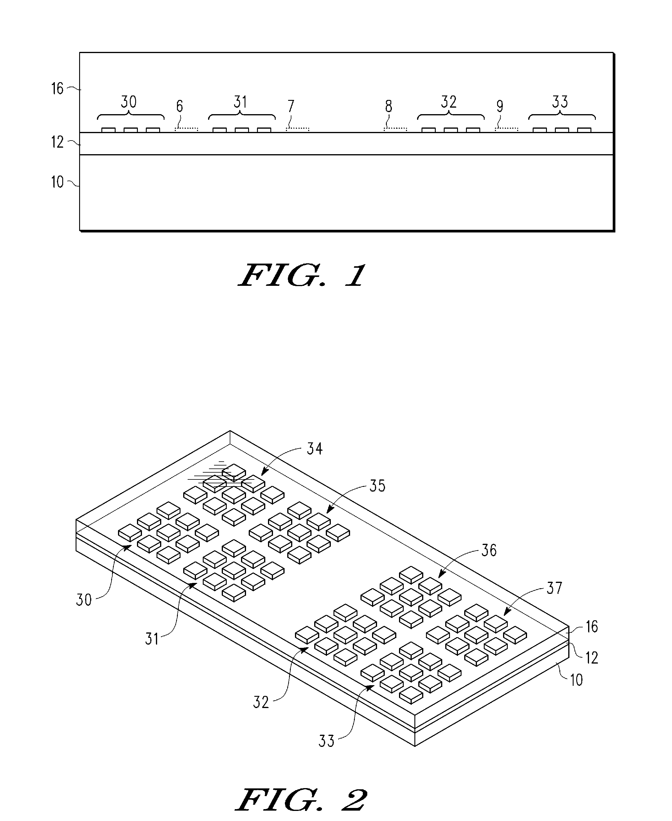
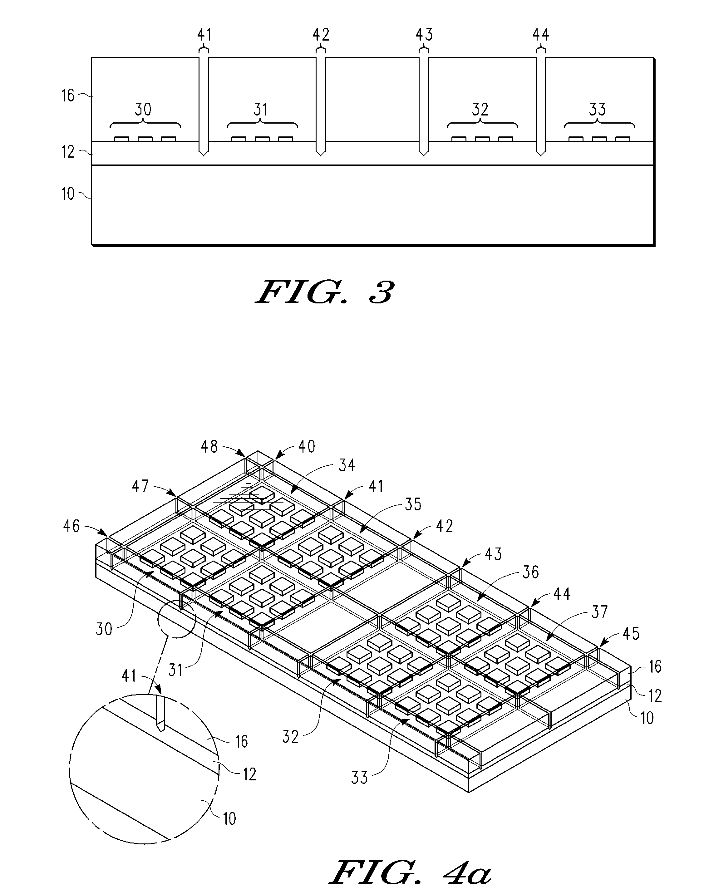
[0030]A method and apparatus are described for fabricating high density encapsulated semiconductor device or devices with integrated shielding. As a preliminary step, a plurality of circuit devices and an optional embedded grounding frame are assembled as a panel by mounting the circuit devices on a process carrier using a removable attachment device, such as a thick double-sided tape or chemical attachment layer. This assembly occurs prior to forming the underlying circuit substrate (also referred to in this application as a layered redistribution structure). Once the circuit devices are affixed to the removable attachment device, the circuit devices are encapsulated with a molding compound or resin. By drilling the molding compound to form via openings between individual circuit device...


PUM


Abstract

Electromagnetic shielding for an integrated circuit packaged device. The method includes forming shielding structures by forming openings in an encapsulated structure. The openings are filled with conductive material that surrounds at least one die. The encapsulated structure may include a plurality of integrated circuit die. A layered redistribution structure is formed on one side of the encapsulated structure.

Description

RELATED APPLICATIONS[0001]This application is a continuation-in-part of U.S. application Ser. No. 11 / 854,776 entitled “Integrated Shielding Process for Precision High Density Module Packaging,” having a common assignee and filed on Sep. 13, 2007, all of which is incorporated by reference in its entirety.BACKGROUND OF THE INVENTION[0002]1. Field of the Invention[0003]This invention relates in general to integrated circuits and more particularly to providing shielding for encapsulated integrated circuits.[0004]2. Description of the Related Art[0005]Some integrated circuits are implemented in packages having electromagnetic shields for protection from electromagnetic interference (EMI). An example of such packages includes multiple chip modules (MCM) which have a plurality of discrete microelectronic devices (e.g., a processor unit, memory unit, related logic units, resistors, capacitors, inductors, and the like) that are connected together on a single MCM substrate. These shielding st...

Claims


Application Information

Patent Timeline
Patent Type & Authority Applications(United States)
IPC IPC(8): H01L21/56
CPCH01L21/561H01L24/19H01L21/6835H01L23/3121H01L23/552H01L24/96H01L24/97H01L25/0655H01L2221/68345H01L2224/92H01L2224/97H01L2924/01013H01L2924/01029H01L2924/0103H01L2924/01033H01L2924/01047H01L2924/01078H01L2924/01079H01L2924/01082H01L2924/09701H01L2924/14H01L2924/15174H01L2924/15311H01L2924/19041H01L2924/19042H01L2924/19043H01L2924/3025H01L21/568H01L2224/04105H01L2224/12105H01L2224/0401H01L2924/014H01L2924/01023H01L2924/01006H01L2224/96H01L2224/82H01L2924/181H01L2223/6677H01L2924/00
Inventor TANG, JINBANGFREAR, DARRELLIN, JONG-KAIMANGRUM, MARC A.BOOTH, ROBERT E.HERR, LAWRENCE N.BURCH, KENNETH R.
Owner NORTH STAR INNOVATIONS
Why Eureka
Try Eureka