Manufacturing method of semiconductor apparatus

a manufacturing method and semiconductor technology, applied in the direction of electrical devices, semiconductor devices, semiconductor/solid-state device details, etc., can solve the problems of increasing reducing the detection accuracy of alignment patterns, and reducing the formation position of wiring patterns with respect to the internal connection terminal b>102/b>, so as to reduce the detection accuracy is sufficient, and the manufacturing cost of the semiconductor apparatus can be reduced.

Inactive Publication Date: 2009-03-19
SHINKO ELECTRIC IND CO LTD
View PDF9 Cites 21 Cited by
  • Summary
  • Abstract
  • Description
  • Claims
  • Application Information

AI Technical Summary

Benefits of technology

[0020]Exemplary embodiments of the present invention provide a manufacturing method of a semiconductor apparatus capable of improving accuracy of a formation position of a wiring pattern with respect to an internal connection terminal and also reducing a manufacturing cost of the semiconductor apparatus and further improving a yield of the semiconductor apparatus.
[0029]According to the invention, a through groove for exposing an alignment pattern formed in a scribe region is disposed in an insulating layer formed on a semiconductor substrate, so that the alignment pattern can be recognized by an exposure apparatus using a CCD camera with sufficient detection accuracy of the alignment pattern without using an exposure apparatus having an infrared or X-ray transmission function with insufficient detection accuracy of the alignment pattern, so that accuracy of a formation position of a wiring pattern with respect to an internal connection terminal can be improved.
[0030]Also, by disposing the through groove for exposing the alignment pattern formed in the scribe region in the insulating layer formed on the semiconductor substrate, the alignment pattern can be recognized by an exposure apparatus using an inexpensive CCD camera without using an expensive exposure apparatus having an infrared or X-ray transmission function, so that a manufacturing cost of a semiconductor apparatus can be reduced.
[0031]Further, by disposing the through groove for exposing the scribe region in the insulating layer formed on the semiconductor substrate, only the semiconductor substrate is cut in a cutting step and a situation in which an interface between a semiconductor chip and a protective film peels is suppressed, so that a yield of the semiconductor apparatus can be improved.
[0032]According to the invention, accuracy of a formation position of a wiring pattern with respect to an internal connection terminal can be improved and also a manufacturing cost of a semiconductor apparatus can be reduced and further a yield of the semiconductor apparatus can be improved.

Problems solved by technology

However, in the manufacturing method of the related-art semiconductor apparatus 100, accuracy of detection of the alignment pattern is not sufficient in the case of using the exposure apparatus having the infrared or X-ray transmission function, so that accuracy of a formation position of the wiring pattern 104 with respect to the internal connection terminal 102 reduces.
Also, the exposure apparatus having the infrared or X-ray transmission function used in the case of forming a resist film for forming the wiring pattern 104 is expensive, so that a manufacturing cost of the semiconductor apparatus 100 increases.

Method used


Image

  • Manufacturing method of semiconductor apparatus
  • Manufacturing method of semiconductor apparatus
  • Manufacturing method of semiconductor apparatus

Examples


first embodiment

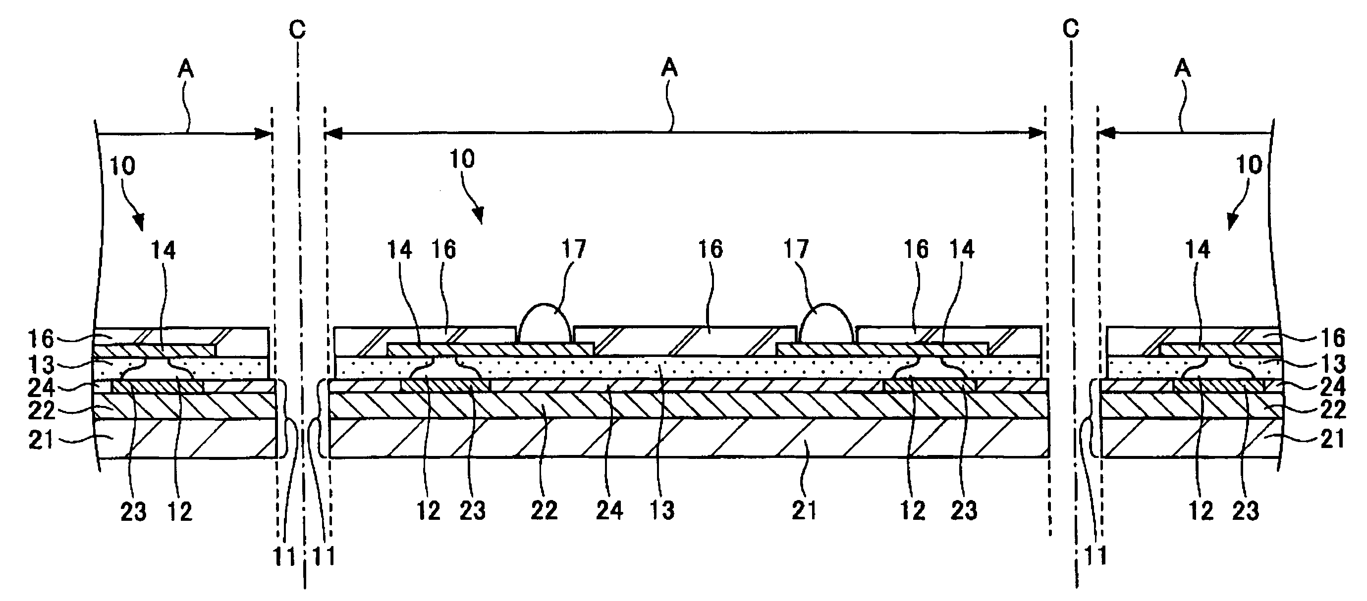
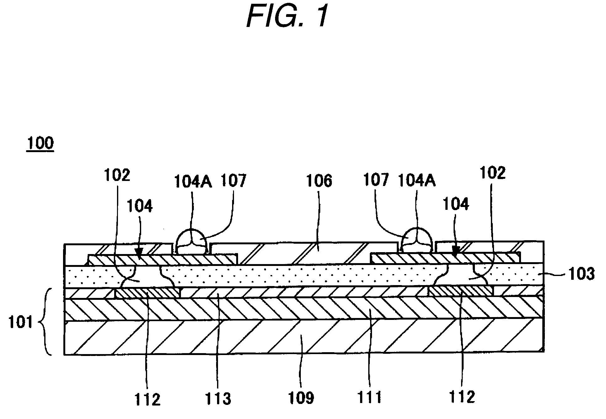
[0080]FIG. 12 is a sectional diagram of a semiconductor apparatus according to a first embodiment of the invention. Referring to FIG. 12, a semiconductor apparatus 10 of the first embodiment has a semiconductor chip 11, internal connection terminals 12, an insulating layer 13, wiring patterns 14, a solder resist 16 and external connection terminals 17.

[0081]The semiconductor chip 11 has a semiconductor substrate 21, a semiconductor integrated circuit 22, plural electrode pads 23 and a protective film 24. The semiconductor substrate 21 is a substrate for forming the semiconductor integrated circuit 22. The semiconductor substrate 21 is formed in a thin plate. A thickness T1 of the semiconductor substrate 21 can be set at, for example, 100 μm to 300 μm. The semiconductor substrate 21 is, for example, a substrate obtained by individualizing an Si wafer formed in a thin plate.

[0082]The semiconductor integrated circuit 22 is disposed on the front side of the semiconductor substrate 21. T...

second embodiment

[0117]FIG. 34 is a sectional diagram of a semiconductor apparatus according to a second embodiment of the invention. In FIG. 34, the same numerals are assigned to the same components as those of the semiconductor apparatus 10 of the first embodiment. Referring to FIG. 34, a semiconductor apparatus 40 of the second embodiment is constructed in a manner similar to the semiconductor apparatus 10 except that a wiring pattern 41 made of a metal seed layer 42 and a metal film 43 is disposed instead of the wiring pattern 14 disposed in the semiconductor apparatus 10 of the first embodiment. As the metal seed layer 42, for example, a Cu layer can be used. Also, a thickness T7 of the metal seed layer 42 can be set at, for example, 0.5 μm to 1.0 μm. As the metal film 43, for example, Cu can be used. Also, a thickness T8 of the metal film 43 can be set at, for example, 10 μm to 20 μm.

[0118]FIGS. 35 to 46 are diagrams showing manufacturing steps of the semiconductor apparatus according to the s...


PUM


Abstract

Alignment patterns are formed in scribe regions of a semiconductor substrate, and through grooves for exposing the scribe regions are disposed in an insulating layer formed on the semiconductor substrate. Formation positions of wiring patterns are aligned based on the alignment patterns, and a metal layer is patterned and the wiring patterns are formed.

Description

TECHNICAL FIELD[0001]The present disclosure relates to a manufacturing method of a semiconductor apparatus. The present disclosure can be applied to a manufacturing method of a semiconductor apparatus in which flip chip bonding between a semiconductor chip and a wiring pattern is made, the semiconductor apparatus having substantially the same size as that of the semiconductor chip in a state of being viewed from the plane.RELATED ART[0002]A related-art semiconductor apparatus includes a semiconductor apparatus (for example, see FIG. 1) called a chip size package formed in substantially the same size as that of a semiconductor chip in a state of being viewed from the plane. FIG. 1 is a sectional diagram of a related-art semiconductor apparatus. Referring to FIG. 1, a related-art semiconductor apparatus 100 has a semiconductor chip 101, internal connection terminals 102, a resin layer 103, wiring patterns 104, a solder resist and external connection terminals 107.[0003]The semiconduct...

Claims


Application Information

Patent Timeline
Patent Type & Authority Applications(United States)
IPC IPC(8): H01L21/304
CPCH01L23/3114H01L2224/0401H01L24/11H01L24/12H01L24/94H01L2223/5442H01L2223/5446H01L2224/0231H01L2224/13099H01L2224/274H01L2924/01013H01L2924/01022H01L2924/01029H01L2924/01033H01L2924/01074H01L2924/01078H01L2924/01079H01L2924/14H01L2924/01005H01L2924/01006H01L2924/01023H01L2924/014H01L2224/02333H01L23/544H01L2224/05624H01L2224/06135H01L2924/00014H01L21/78H01L23/48
Inventor MACHIDA, YOSHIHIRO
Owner SHINKO ELECTRIC IND CO LTD
Why Eureka
Try Eureka