Electro-optical device and electronic apparatus including the same

a technology of optical devices and electronic devices, applied in the direction of static indicating devices, instruments, etc., can solve the problems of complicated configuration of pixel circuits provided in each pixel for driving liquid crystal, deteriorating and affecting the display performance of liquid crystal devices

Inactive Publication Date: 2009-03-26
JAPAN DISPLAY WEST
View PDF1 Cites 34 Cited by
  • Summary
  • Abstract
  • Description
  • Claims
  • Application Information

AI Technical Summary

Benefits of technology

[0009]An advantage of some aspects of the invention is that it provides an electro-optical device capable of compensating for lowering of a potential of a pixel electrode due to a pushdown phenomenon occurring when a pixel-switching TFT is switched from a selection state to a non-selection state, that is, insufficient writing of an image signal, and an electronic apparatus, such as a display device, including the electro-optical device.

Problems solved by technology

Due to the pushdown phenomenon, the potential of the pixel electrode, which is set by the image signal to be supplied to the pixel electrode, is lowered, and accordingly display performance of the liquid crystal device is deteriorated.
In such a liquid crystal device, the lowering of the potential of the pixel electrode has a direct effect on the luminance of the pixel, and significantly deteriorates the display performance of the liquid crystal device.
In the technology disclosed in JP-A-2002-341313, there is a problem in that the configuration of a pixel circuit provided in each pixel for driving liquid crystal is complicated.
In addition, when the pixel is reduced in size to allow high-definition images to be displayed in the display region, it is difficult to ensure a space in the pixels in which to dispose the TFTs and wiring lines connecting the TFTS.
If the TFTs and the wiring lines can be formed in the pixels, the potential of the pixel electrode may be lowered due to parasitic capacitance between the element, such as the TFT, and the wiring line, and the image signal may be insufficiently written to the pixel electrode.
For this reason, it becomes technically difficult to ensure a period in which the precharge operation is to be executed.
For this reason, adjustment of the potential of the image signal becomes complicated, and the configuration of the external circuit, which executes such adjustment, also becomes complicated.
For this reason, even if the image signal is supplied to the driving electrode through the data line and the driving transistor element while the driving transistor element is in the selection state, it becomes difficult to maintain the electrode potential of the driving electrode at a potential according to the image signal.
For this reason, it becomes difficult to maintain the electrode potential due to the second change corresponding to the change in the electrode potential.

Method used


Image

  • Electro-optical device and electronic apparatus including the same
  • Electro-optical device and electronic apparatus including the same
  • Electro-optical device and electronic apparatus including the same

Examples


first embodiment

[0114]First, an embodiment of an electro-optical device according to the invention will be described with reference to FIGS. 1 to 12.

Overall Configuration of Electro-Optical Device

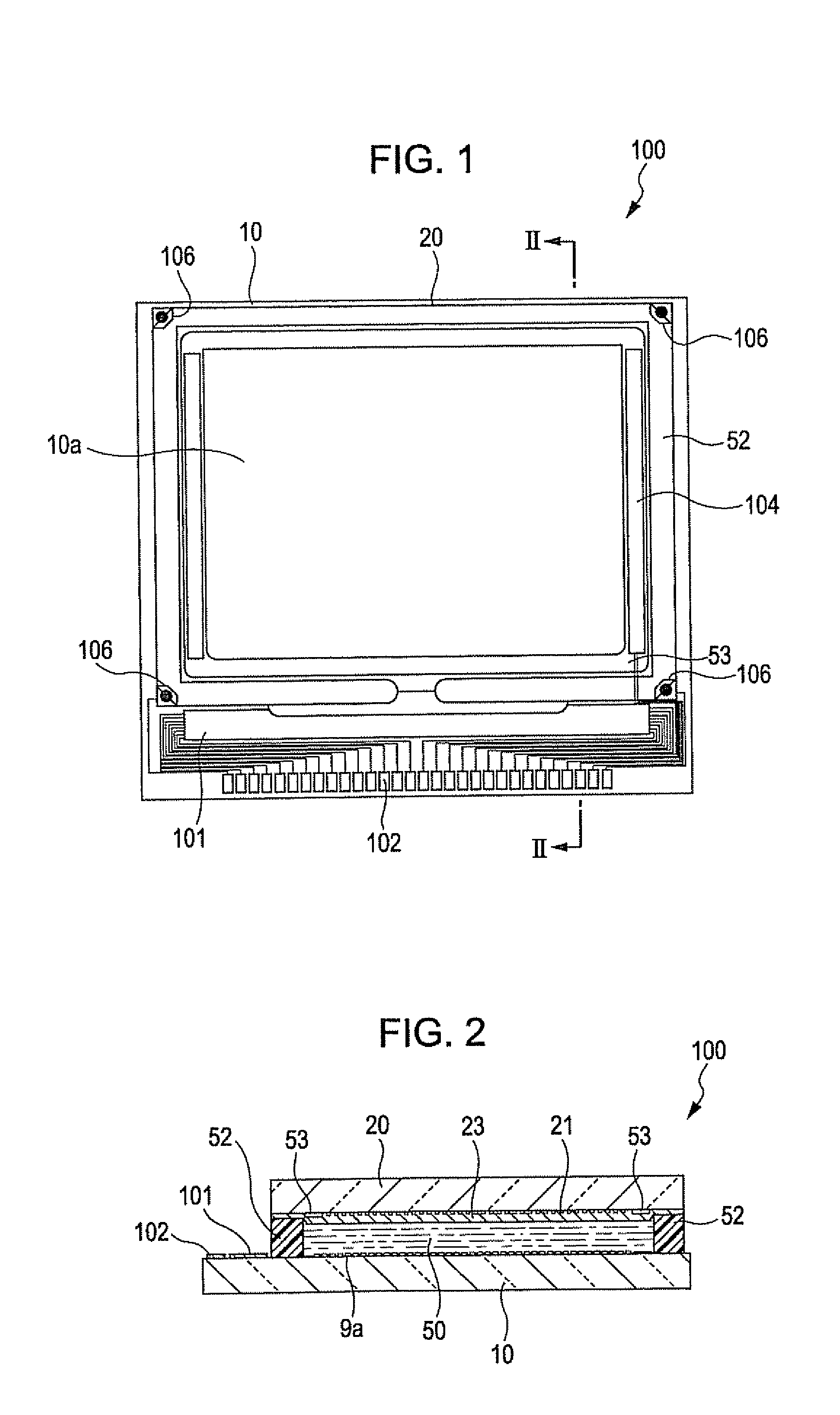
[0115]The overall configuration of a liquid crystal panel 100 as an embodiment of an electro-optical device according to the invention will be described with reference to FIGS. 1 and 2. FIG. 1 is a schematic plan view of a liquid crystal panel 100 serving as a TFT array substrate is viewed from a counter substrate side, together with the constituent elements formed thereon. FIG. 2 is a sectional view taken along the line II-II of FIG. 1. Here, a TFT active matrix driving type liquid crystal panel equipped with a driving circuit is exemplified.

[0116]Referring to FIGS. 1 and 2, in the liquid crystal panel 100 of this embodiment, a TFT array substrate 10 and a counter substrate 20 are disposed to be opposed to each other. A liquid crystal layer 50 is filled between the TFT array substrate 10 and the counter s...

second embodiment

Electrical Configuration of Electro-Optical Device

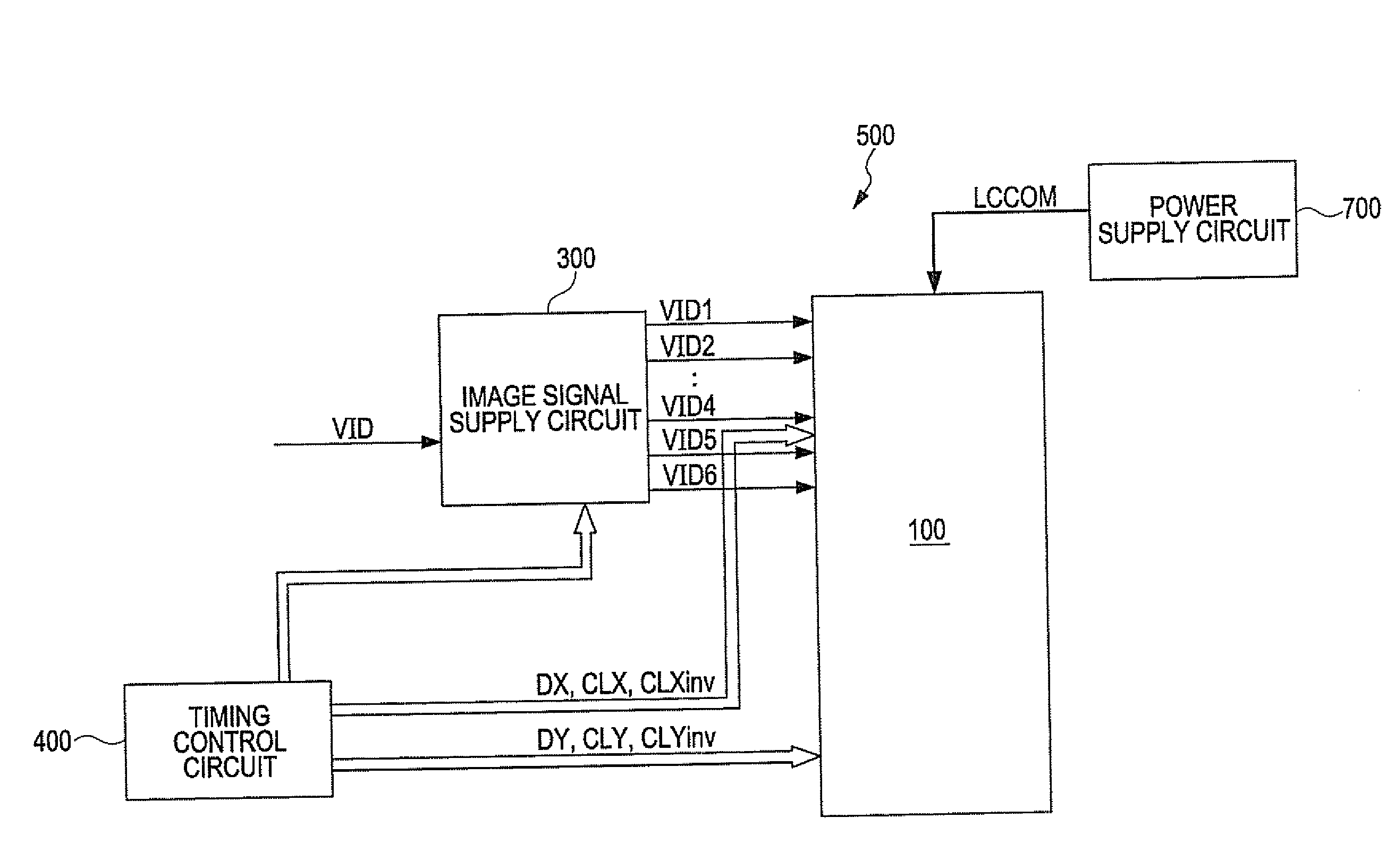
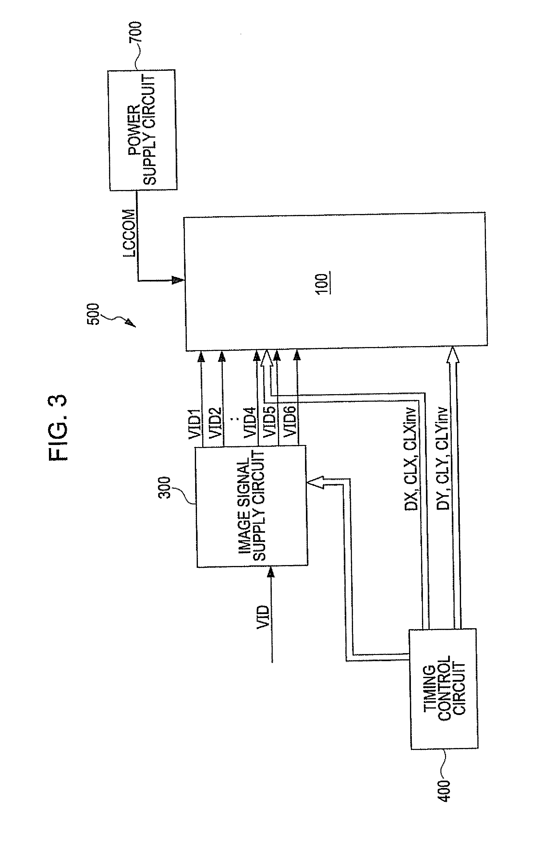
[0187]Next, an embodiment of an electro-optical device according to the invention and an electronic apparatus according to the invention will be described with reference to FIGS. 13 to 27. FIG. 13 is a block diagram showing the overall configuration of a liquid crystal device including a liquid crystal panel 100a. FIG. 14 is a block diagram showing the electrical configuration of the liquid crystal panel 100a.

[0188]An electro-optical device of this embodiment is a liquid crystal device which is the same as the electro-optical device of the first embodiment. Therefore, as for the electro-optical device of this embodiment, the same parts as those in the above-described liquid crystal device are represented by the same reference numerals, and detailed descriptions thereof will be omitted. As for the parts represented by the same reference numerals as the above-described liquid crystal device, when a part performs a different operation ...


PUM


Abstract

An electro-optical device includes a pixel circuit with a driving transistor element, a storage capacitor, and a capacitive element. The driving transistor element is electrically connected to a corresponding data line and a corresponding driving electrode. The storage capacitor is electrically connected to the driving transistor element and the driving electrode. The storage capacitor holds an image signal supplied through the corresponding data line as potential at the driving electrode. The capacitive element is electrically connected to the driving transistor element and the driving electrode. The capacitive element compensates for a change in the potential of the driving electrode when the driving transistor element is switched from a selection state to a non-selection state. The capacitive element is supplied with a correction signal that defines timing at which the potential of the capacitive element is controlled.

Description

BACKGROUND[0001]1. Technical Field[0002]The present invention relates to an electro-optical device, such as a liquid crystal device, and an electronic apparatus, such as a liquid crystal projector, including the electro-optical device.[0003]2. Related Art[0004]A liquid crystal device that is an example of an electro-optical device of this type includes a plurality of scanning lines and a plurality of data lines arranged vertically and horizontally in a display region having a plurality of pixels, and a plurality of pixel electrodes at intersections between the scanning lines and the data lines. The liquid crystal device is of an active matrix drive type in which pixel-switching TFTs (Thin Film Transistors) provided to correspond to the pixels are turned on / off, that is, are switched between a selection state and a non-selection state in accordance with scanning signals, and image signals are supplied from the data lines to the pixel electrodes through the pixel-switching TFTs, there...

Claims


Application Information

Patent Timeline
Patent Type & Authority Applications(United States)
IPC IPC(8): G09G3/36
CPCG09G3/3655G09G2320/0219G09G2300/0852G09G3/3659
Inventor WATANABE, KENYA
Owner JAPAN DISPLAY WEST
Why Eureka
Try Eureka