

Liquid crystal display device
- Summary
- Abstract
- Description
- Claims
- Application Information
AI Technical Summary
Benefits of technology
Problems solved by technology
Method used
Image

Examples
exemplary embodiment 1
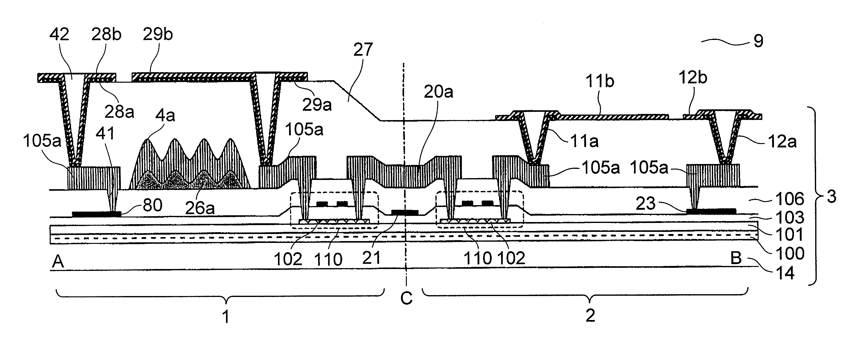
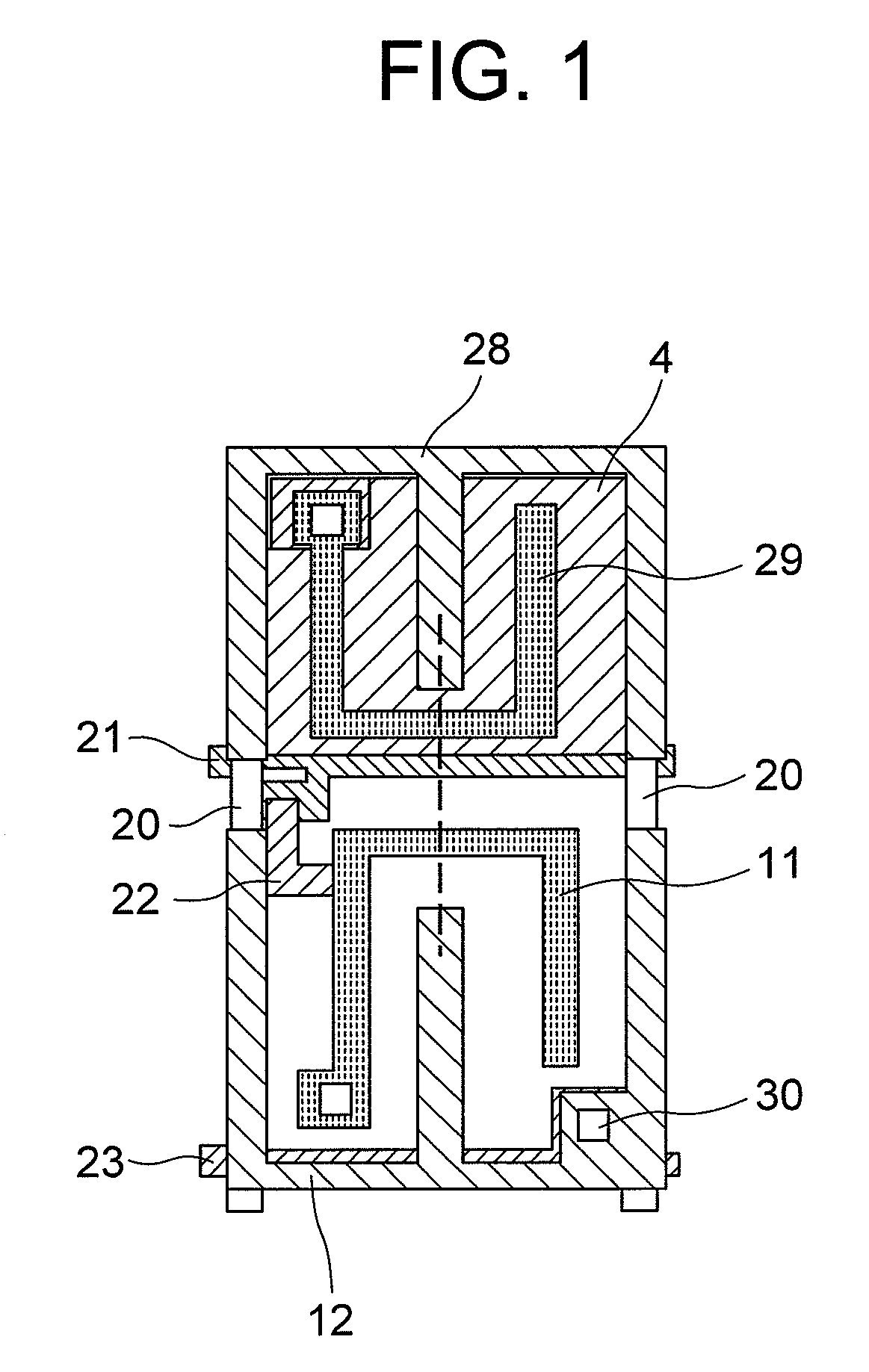
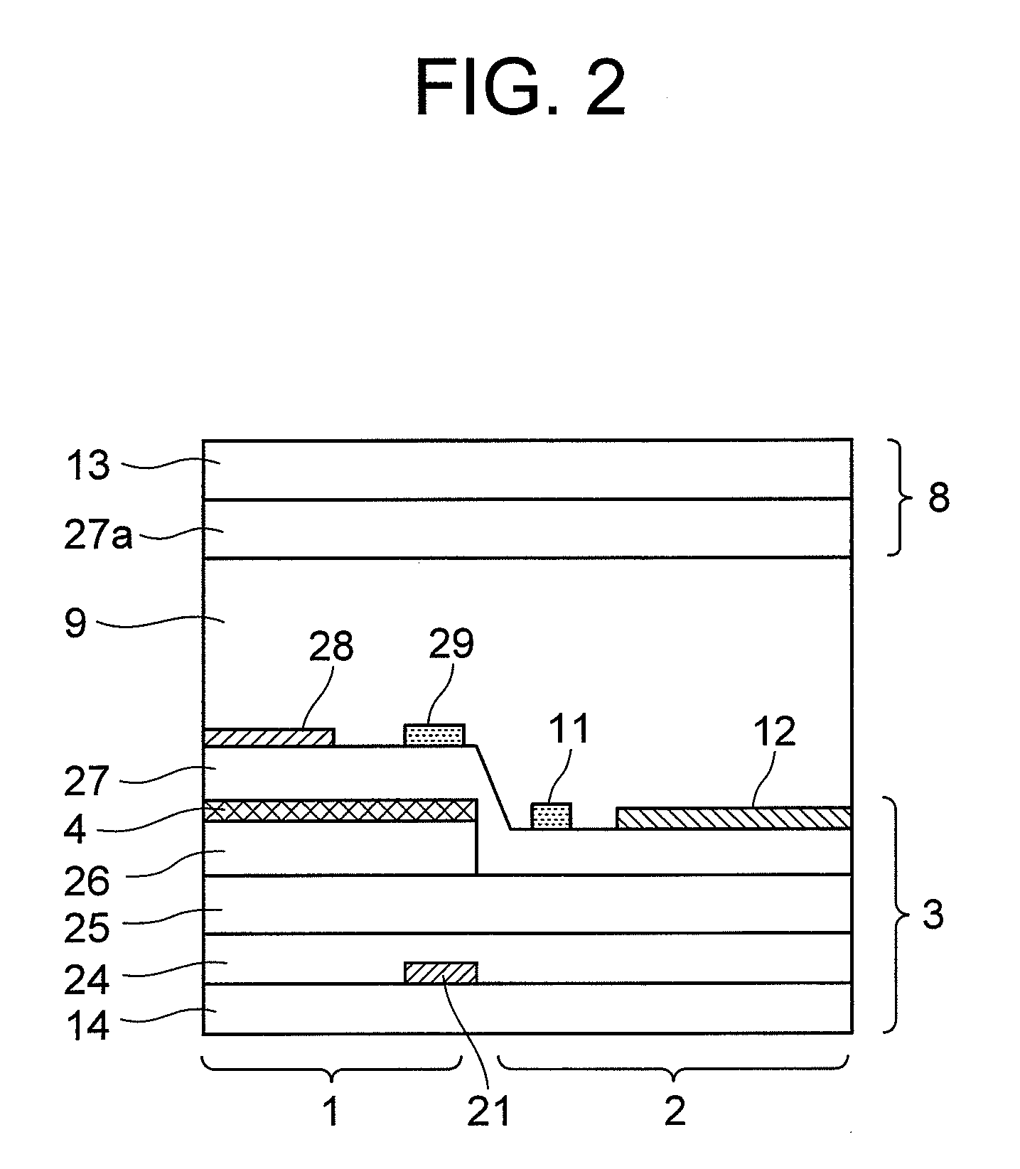
[0080]FIG. 1 is a plan view showing a unit pixel that forms a liquid crystal panel of a liquid crystal display device according to an exemplary embodiment 1 of the invention, and FIG. 2 is a sectional view taken along a dotted line of the unit pixel shown in FIG. 1.
[0081]As shown in FIG. 1 and FIG. 2, the unit pixel that forms the liquid crystal panel of the liquid crystal display device according to the exemplary embodiment 1 of the invention has the reflection area 1 and the transmission area 2, and the corresponding ranges are being sectioned by data lines 20 and scanning lines 21 that are provided in matrix on the whole surface of the liquid crystal panel.
[0082]First, the lower substrate 3 will be described. The lower substrate 3 is formed with laminated parts each having various functions mainly for driving displaying members. On an insulating film deposited on a glass substrate 14, provided are the scanning lines 21 to which scanning signals are inputted, the data lines 20 to ...
exemplary embodiment 2
Effects of Exemplary Embodiment 2
[0117]In the exemplary embodiment 2 of the invention, the reflection common electrode 28, the reflection pixel electrode 29, the transmission common electrode 12″, and the transmission pixel electrode 11″ are formed simultaneously. Thus, the number of manufacturing steps can be reduced.
[0118]When the reflection common electrode and the reflection pixel electrode are formed with a non-transparent electric conductor such as Mo and the transmission common electrode and the transmission pixel electrode are formed with a transparent electric conductor such as ITO, it is necessary to carry out a series of steps twice (the steps including sputtering, applying resist, exposure, development, etching, and exfoliating resist). However, the exemplary embodiment 2 requires the steps only once, which results in reducing the manufacturing time and manufacturing cost.
[0119]While the effect regarding the numerical aperture achieved by reducing the junction between th...
exemplary embodiment 3
Effects of Exemplary Embodiment 3
[0128]As a reason for causing light leakage at the time of dark state in the reflection area 1, reflection of the incident light on the reflection common electrode 28 and the reflection pixel electrode 29 can also be considered. As described in the effects of the exemplary embodiment 1, a proper lateral electric field is not generated in the liquid crystal layer 9 on the reflection common electrode 28 and the reflection pixel electrode 29, so that the liquid crystal molecules are not rotated for providing dark state. Thus, the following light exhibits no change in the polarized state to provide dark state (the light that passes through the liquid crystal layer 9 on the reflection common electrode 28 and the reflection pixel electrode 29, reflected on the reflection common electrode 28 and the reflection pixel electrode 29, and passes again through the liquid crystal layer 9 on the reflection common electrode 28 and the reflection pixel electrode 29; ...
PUM
 Abstract
Description
Claims
Application Information