Trench MOSFET with thick bottom oxide tub

a technology of oxide tubing and mosfet, which is applied in the direction of semiconductor devices, electrical equipment, basic electric elements, etc., can solve the problems of undesirable thick oxide layer formed near the bottom of the trench, adversely increasing power consumption, etc., and achieves the effect of increasing the on-resistance of the mosfet device and reducing the gate-to-drain capacitan

Inactive Publication Date: 2009-04-02
FORCE MOS TECH CO LTD
View PDF4 Cites 28 Cited by
  • Summary
  • Abstract
  • Description
  • Claims
  • Application Information

AI Technical Summary

Benefits of technology

[0007]It is therefore an aspect of the present invention to provide a new and improved semiconductor power device by forming a thick oxide layer at a narrower and deeper trench below the normal trench gate. Such Y-shaped oxide layer structure can significantly re

Problems solved by technology

However, a thicker oxide layer formed at the trench bottom may also cause the on-resistance of the semiconductor power device to increase in the meantime thus adversely increasing the power con

Method used


Image

  • Trench MOSFET with thick bottom oxide tub
  • Trench MOSFET with thick bottom oxide tub
  • Trench MOSFET with thick bottom oxide tub

Examples


Embodiment Construction

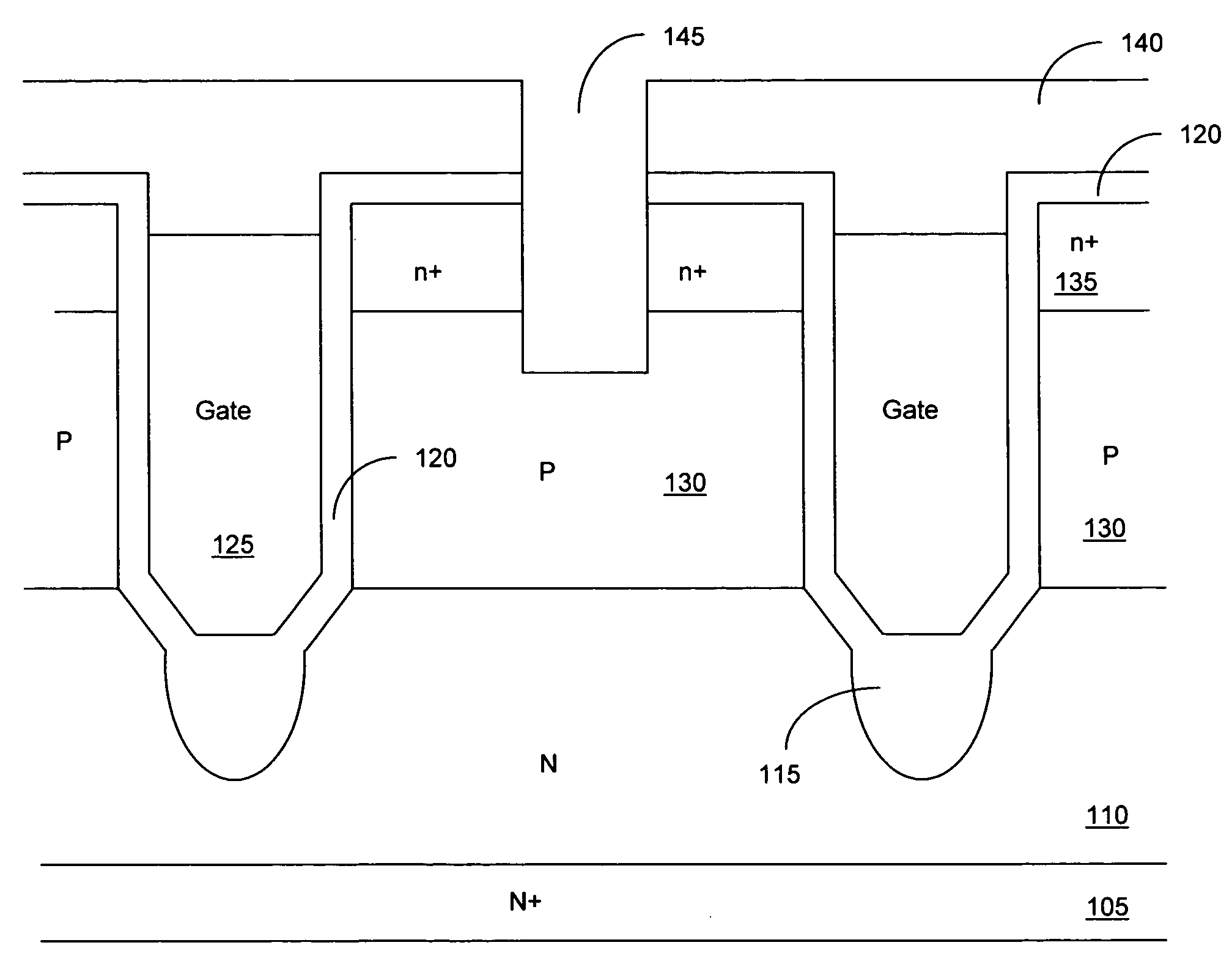
[0018]Referring to FIG. 2 for a side cross sectional view of a MOSFET device 100 formed on a N+ substrate 105 supporting an epitaxial layer 110 with trenched polysilicon gates 125. The trenched gates 125 are padded by a gate oxide layer 120 and surrounded by P-body regions 130. The body regions further encompassed source regions 135 formed near the top surface of the epitaxial layer 110 surrounding the trenched gate 125. An oxide insulation layer covering the top surface with contact trenches open through the insulation layer filled with Ti / TiN / W as contact plug inside the contact trenches 145 to contact the source / body regions and the trench contacts to contact the gate (not shown). A top metal layer 150 is formed on top of the trench contacts 145 and patterned into source metal 150 and gate pads (not shown). The MOSFET device has a special oxide layer 115 below the trenched gate 125 formed with a tub shape having a narrow width than the trenched gates 125 thus constituting a Y-sha...


PUM


Abstract

A semiconductor power device includes a plurality of trenched gates. The trenched gates include a thin dielectric layer padded sidewalls of the trenched gate and a tub-shaped thick dielectric layer below a bottom of the trenched gates having a width narrower than the trenched gate. In an exemplary embodiment, the tub-shaped thick dielectric layer below a bottom of the trenched gates further includes a local deposition of silicon oxide (LOCOS) filling in a tub-shaped trench having a narrower width than the trenched gate. In another exemplary embodiment, the tub-shaped thick dielectric layer below a bottom of the trenched gates further comprising a high density plasma (HDP) chemical vapor deposition (CVD) silicon oxide filled in a tub-shaped trench having a narrower width than the trenched gate.

Description

BACKGROUND OF THE INVENTION[0001]1. Field of the Invention[0002]The invention relates generally to the device configuration and manufacturing methods for fabricating the semiconductor power devices. More particularly, this invention relates to an improved and novel manufacturing process and device configuration for providing the MOSFET device with thick oxide bottom tub for reducing the gate-drain capacitance[0003]2. Description of the Related Art[0004]In order to increase the switching speed of a semiconductor power device, it is desirable to reduce the gate to drain capacitance Crss. A thick oxide formed at the trench bottom of the trench gate is frequently implemented to reduce the gate to drain capacitance. However, a thicker oxide layer formed at the trench bottom may also cause the on-resistance of the semiconductor power device to increase in the meantime thus adversely increasing the power consumptions due to a higher on-resistance.[0005]FIG. 1A shows a standard MOSFET devic...

Claims


Application Information

Patent Timeline
IPC IPC(8): H01L29/94H01L21/336
CPCH01L29/0878H01L29/41766H01L29/4236H01L29/7813H01L29/456H01L29/66727H01L29/66734H01L29/42368
Inventor HSHIEH, FWU-IUAN
Owner FORCE MOS TECH CO LTD
Why Eureka
Try Eureka