Bank Structure for a Display Panel and Method of Manufacturing the Same

Inactive Publication Date: 2009-04-02
AU OPTRONICS CORP
View PDF4 Cites 2 Cited by
  • Summary
  • Abstract
  • Description
  • Claims
  • Application Information

AI Technical Summary

Benefits of technology

[0010]One objective of this invention is to provide a bank structure for a display panel, wherein the display panel comprises a substrate. The bank structure is formed on the surface of the substrate. The bank structure comprises a periphery and a partition. The periphery and the substrate both form a receiving space, into which the partition divides the receiving space into a first sub-space and a second sub-space in fluid communication with each other. When dropped into the receiving space, ink will fill into the first sub-space and the second sub-space. In this way, ink will be distributed uniformly in the receiving space, thus improving the ink injection precision and injection dose accuracy and prevent ink overflow and consequent color mixtures with the adjacent pixels. Furthermore, the extension of the receiving space may also mitigate the central protrusion of an ink drop in a limited space due to the surface tension and cohesion.

Problems solved by technology

Unfortunately, when the ink is dropped into the receiving space formed by the bank, a small volume of the receiving space or discontinuous and asymmetric areas of the receiving space that are divided by common electrodes or other electrodes often lead to poor injection precision and poor injection dose accuracy.
This tends to cause underfilling or an ink drop to protrude in the center portion thereof, thereby making the edges or corners of the receiving space devoid of ink.
Also possibly, the incorrect injecting locations or ununiform injection dose may even cause ink to overflow and mix with the ink of other colors in the adjacent pixels, thus resulting in a decreased yield.
It follows from the above description that because of the poor ink injection precision and poor injection dose accuracy in producing color filters by ink injection, there is still no bank structure that can prevent these problems.

Method used


Image

  • Bank Structure for a Display Panel and Method of Manufacturing the Same
  • Bank Structure for a Display Panel and Method of Manufacturing the Same
  • Bank Structure for a Display Panel and Method of Manufacturing the Same

Examples


Embodiment Construction

[0023]The following embodiments and attached drawings are intended to illustrate rather than to limit this invention. It should be noted that the elements unrelated to this invention have been omitted from depiction in the following embodiments and attached drawings.

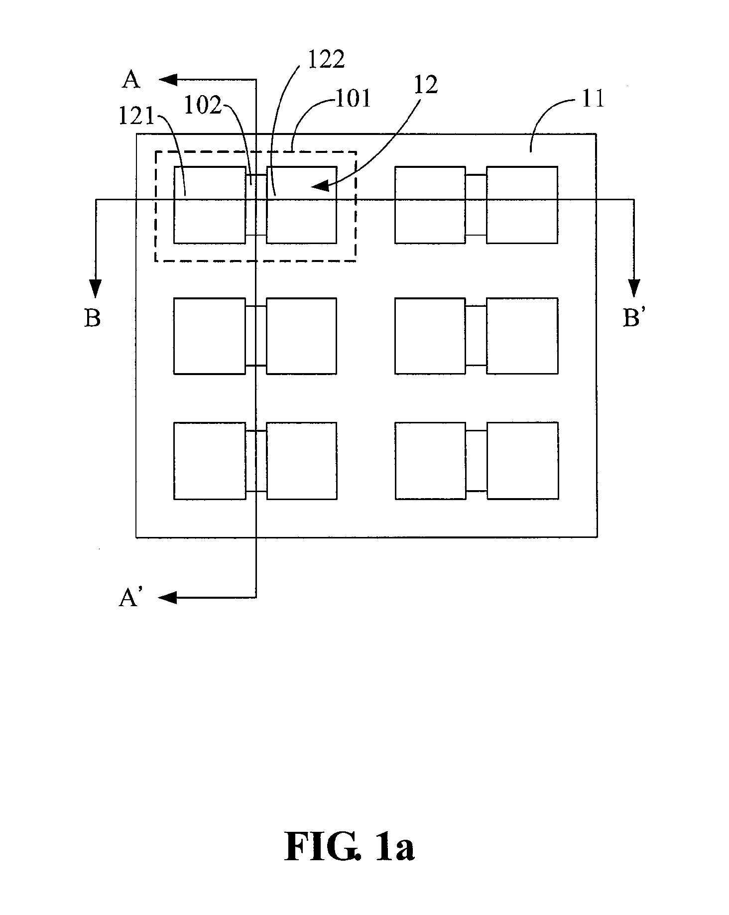
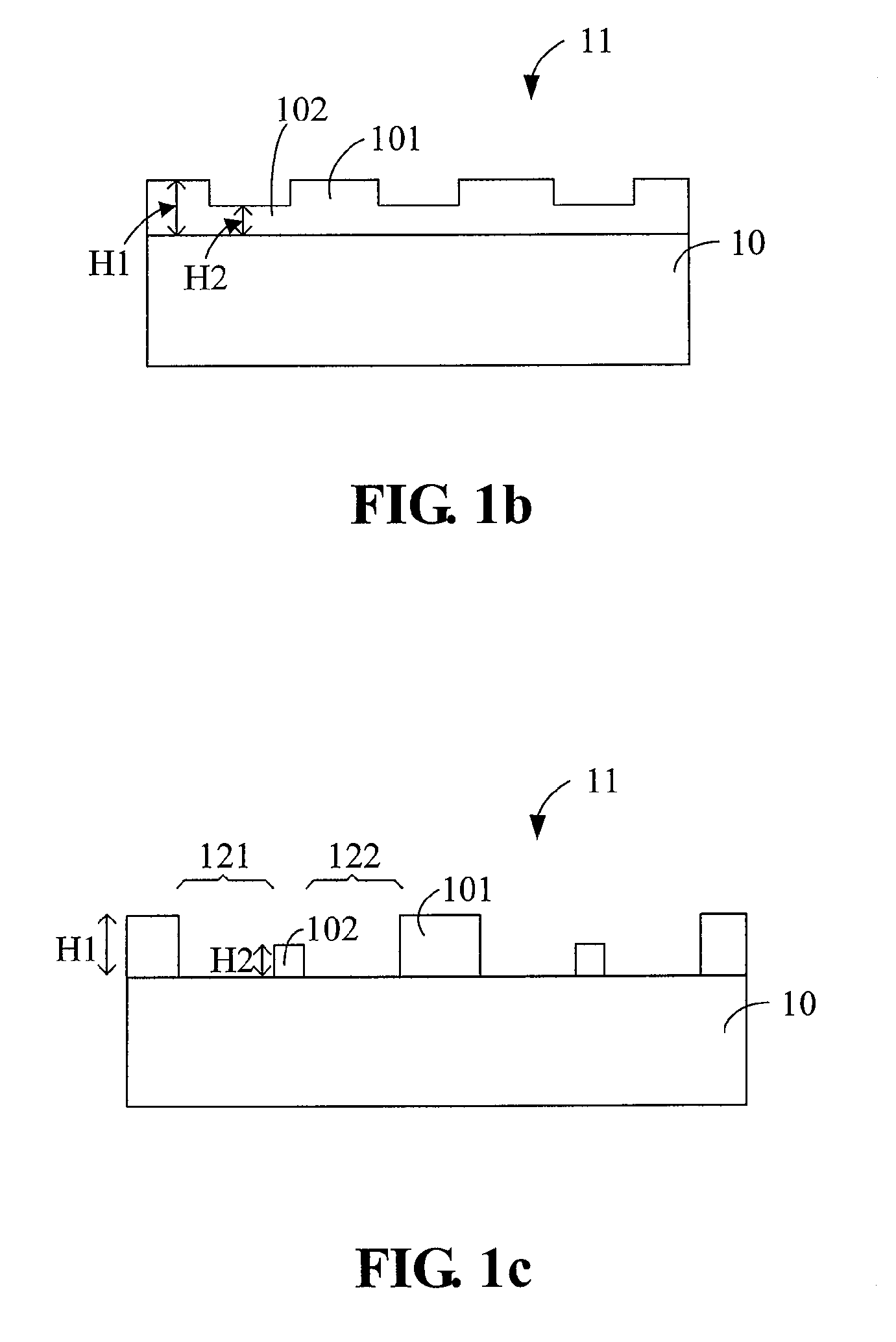
[0024]FIG. 1a illustrates a bank structure 11 of this invention when applied in a display panel, while FIG. 1b and FIG. 1c illustrate a cross-sectional view of a portion of the bank structure 11 respectively. More specifically, FIG. 1b is a cross-sectional view taken along line A-A′ in FIG. 1a, while FIG. 1b is a cross-sectional view taken along line B-B′ in FIG. 1a.

[0025]The bank structure 11 depicted in FIG. 1a is formed on a substrate 10, and comprises a periphery 101 and a partition 102. The periphery 101 forms a receiving space 12, into which the partition 102 is disposed. In FIG. 1a, identical depictions represent identical structures. In other words, FIG. 1a depicts a plurality of receiving spaces, each of which ...


PUM


Abstract

A bank structure for a display panel is provided. The display panel comprises a substrate, and the bank structure is formed on the surface of the substrate. The bank structure comprises a periphery and a partition, wherein the periphery forms a receiving space with the substrate and the partition is disposed in the receiving space for separating the receiving space into two sub-spaces with fluid-communication. Therefore, the ink can be injected and uniformly distributed in the sub-spaces to overcome the disadvantages of poor injection precision and increasing the spray control of the ink.

Description

[0001]This application claims the benefit from the priority of Taiwan Patent Application No. 096136762, filed on Oct. 1, 2007, the contents of which are herein incorporated by reference in their entirety.CROSS-REFERENCES TO RELATED APPLICATIONS[0002]Not applicable.BACKGROUND OF THE INVENTION[0003]1. Field of the Invention[0004]The present invention relates to a bank structure for a display panel. More particularly, the present invention relates to a bank structure capable of improving ink distribution for a display panel.[0005]2. Descriptions of the Related Art[0006]Conventionally, a widely adopted method for manufacturing a large color filter is the pigment dispersed method. According to this method, a black photo-resist containing carbon is applied onto a glass substrate using a photo process, and then subjected to a series of processes such as soft baking, exposure, development and hard baking, thereby, forming a black matrix on the substrate as a bank structure to shield light. ...

Claims


Application Information

Patent Timeline
IPC IPC(8): G02B5/20G02B5/00G02B1/00
CPCG02B5/201G02F2001/136236G02F1/133516G02B5/223G02F1/136236
Inventor TSAI, LUNCHEN, CHI-SHENGLUNG, PO-HUAWU, WEN-BIN
Owner AU OPTRONICS CORP
Why Eureka
Try Eureka