Circuit device and method of manufacturing the same

Active Publication Date: 2009-04-02
SEMICON COMPONENTS IND LLC
View PDF50 Cites 65 Cited by
  • Summary
  • Abstract
  • Description
  • Claims
  • Application Information

AI Technical Summary

Benefits of technology

[0010]It is thus an object of the present invention to provide a circuit device, in which circuit elements incorporated therein are electricall

Problems solved by technology

However, it is difficult to provide a plurality of substrates 101 inside the case member 111 in this manner

Method used


Image

  • Circuit device and method of manufacturing the same
  • Circuit device and method of manufacturing the same
  • Circuit device and method of manufacturing the same

Examples


Embodiment Construction

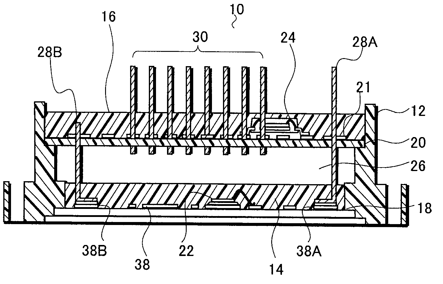
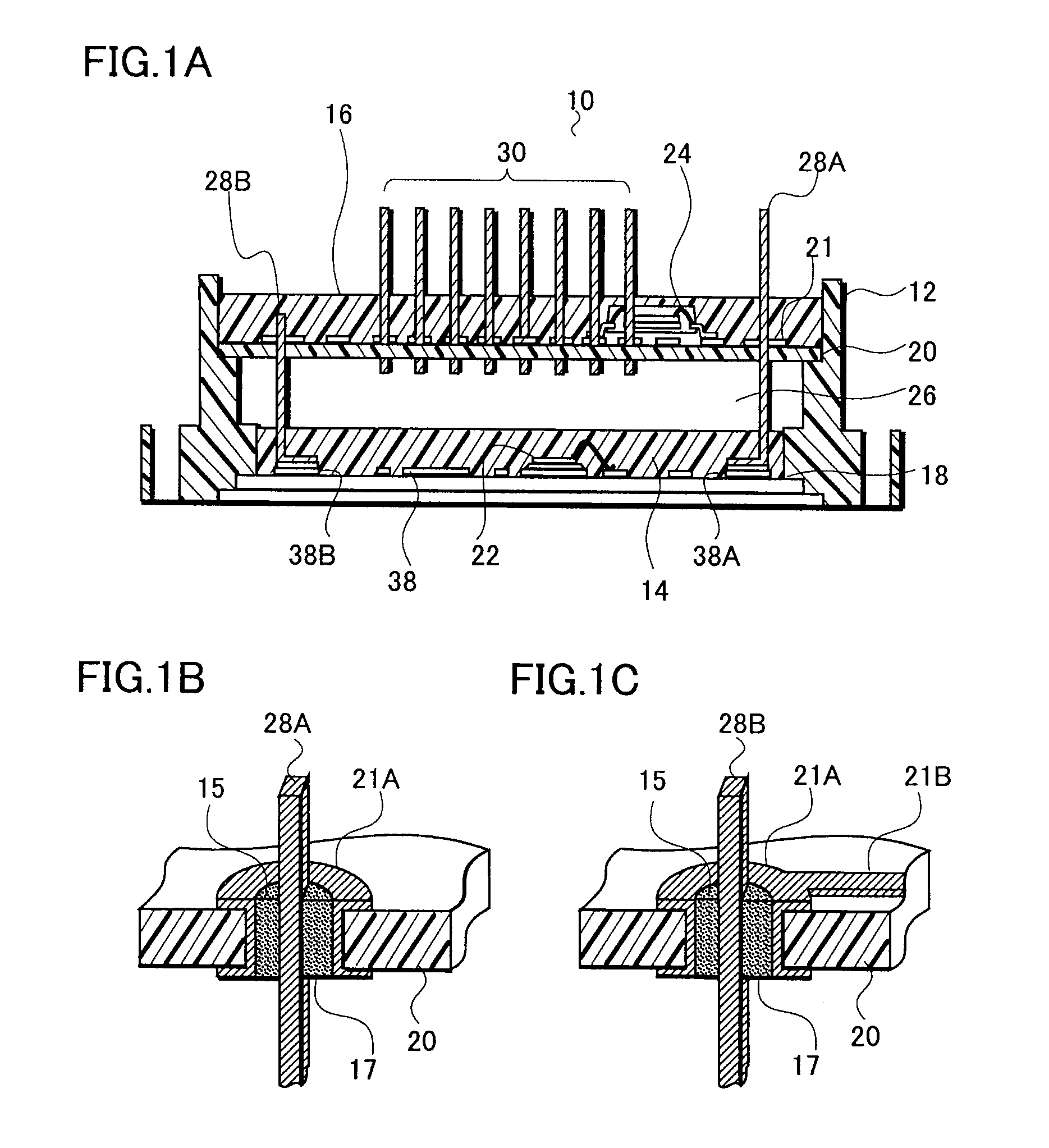
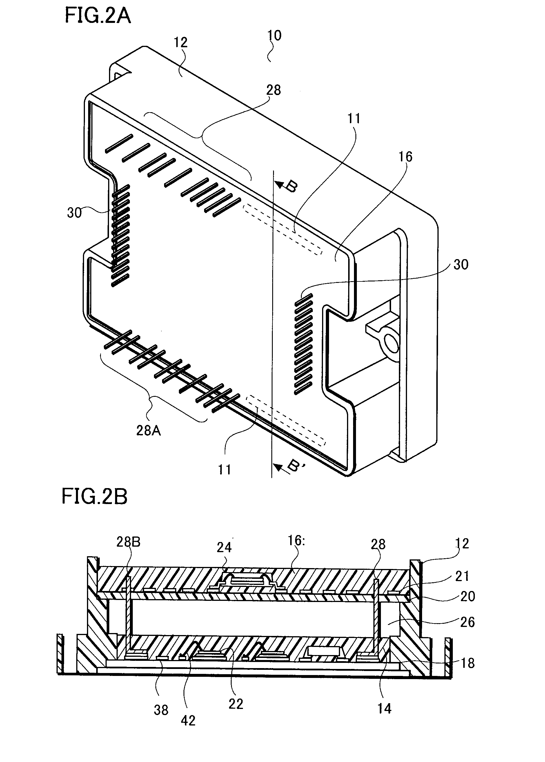
[0025]As an example of the circuit device, the configuration of a hybrid integrated circuit device 10 is described with reference to FIGS. 1A to 1C. FIG. 1A is a cross sectional view of the hybrid integrated circuit device 10, FIG. 1B is a perspective view showing a part of a second circuit board 20 which a lead 28A penetrates, and FIG. 1C is a perspective view showing a part of the second circuit board 20 which a lead 28B penetrates.

[0026]As shown in FIG. 1A, in the hybrid integrated circuit device 10, a first circuit board 18 and a second circuit board 20 are incorporated into a case member 12 in a way that a first circuit board 18 is overlaid with a second circuit board 20. A first circuit element 22 (a power transistor, for example) is arranged on the upper face of the first circuit board 18, and a second circuit element 24 (a microcomputer, for example) is arranged on the upper face of the second circuit board 20. In addition, the leads 28A, 28B are fixedly secured to the first...


PUM

PropertyMeasurementUnit
Electrical conductoraaaaaaaaaa

Abstract

Provided is a circuit device, in which circuit elements incorporated are electrically connected to each other via a lead so as to achieve both of the enhanced functionality and miniaturization. In a hybrid integrated circuit device, a first circuit board and a second circuit board are incorporated into a case member in a way that a first circuit board is overlaid with a second circuit board. A first circuit element is arranged on the upper face of the first circuit board and a second circuit element is arranged on the upper face of the second circuit board. Leads provided in the hybrid integrated circuit device include a lead connected only to the first circuit element mounted on the first circuit board, a lead connected only to the second circuit element mounted on the second circuit board, and a lead connected to both of the first circuit element and the second circuit element.

Description

[0001]This application claims priority from Japanese Patent Application Number JP 2007-250485, filed on Sep. 27, 2007, and JP 2007-284348 filed on Oct. 31, 2007, the content of which is incorporated herein by reference in its entirety.BACKGROUND OF THE INVENTION[0002]1. Field of the Invention[0003]The present invention relates to a circuit device and a method of manufacturing the same, and in particular, relates to a circuit device, in which a hybrid integrated circuit formed on an upper face of a circuit board is sealed with a case member, and a method of manufacturing the same.[0004]2. Description of the Related Art[0005]The configuration of a hybrid integrated circuit device 150 employing a case member 111 is described with reference to FIG. 11. The hybrid integrated circuit device 150 includes: a substrate 101 made of a metal, such as aluminum; an insulating layer 102 formed so as to cover the upper face of the substrate 101; a conductive pattern 103 formed on the upper face of ...

Claims


Application Information

Patent Timeline
IPC IPC(8): H05K7/06H05K3/36
CPCH05K1/144H01L2924/1305H05K3/3447H05K7/1432H05K2201/042H05K2201/10166H05K2201/10303H05K2201/10318H05K2201/10689H05K2201/2018H01L2924/3025H05K3/284H01L2924/13055H01L2924/19107Y10T29/49126H01L2224/48091H01L2224/73265H01L2924/00014H01L2924/00H01L2224/2612H05K7/14322
Inventor SAKAMOTO, HIDEYUKISAITO, HIDEFUMIKOIKETSUKIZAWA, MASAO
Owner SEMICON COMPONENTS IND LLC
Why Eureka
Try Eureka