Through-wafer interconnects for photoimager and memory wafers

a technology which is applied in the field of imager and memory wafer, can solve the problems of limited ability to attach the cover glass on the imager wafer at the wafer level, limit the ability to stack memory and imager devices, etc., and achieve the effects of reducing circuit parasitics (e.g., l and r), increasing volumetric density and device functionality, and reducing the size of the die packag

Inactive Publication Date: 2007-11-27
ROUND ROCK RES LLC
View PDF107 Cites 168 Cited by
  • Summary
  • Abstract
  • Description
  • Claims
  • Application Information

AI Technical Summary

Benefits of technology

[0004]The present invention addresses the shortcomings described above and provides in disclosed exemplary embodiments a through-wafer interconnect for imager, memory and other integrated circuit applications, thereby eliminating the need for wire bonding, making devices incorporating such interconnects stackable to allow increased volumetric density and device functionality and enabling WLP for imager devices. Further, a smaller and more reliable die package is achieved and circuit parasitics (e.g., L and R) are reduced due to the reduced signal path lengths.

Problems solved by technology

A disadvantage of direct bond pad connection on the top side of the die, as depicted in FIG. 1, includes the fact that they sometimes require a wire bond 160 to be electrically connected to a lead frame or other structure for final die packaging.
As a result, this limits the ability to stack memory and imager devices.
Furthermore, the ability to attach the cover glass on imager wafers at the wafer level is limited due to the requirement to make contact to the bond pad on the top side of the wafer.

Method used


Image

  • Through-wafer interconnects for photoimager and memory wafers
  • Through-wafer interconnects for photoimager and memory wafers
  • Through-wafer interconnects for photoimager and memory wafers

Examples


Embodiment Construction

[0041]In the following detailed description, reference is made to the accompanying drawings which form a part hereof, and in which is shown by way of illustration specific embodiments in which the invention may be practiced. These embodiments are described in sufficient detail to enable those of ordinary skill in the art to make and use the invention, and it is to be understood that structural, logical or procedural changes may be made to the specific embodiments disclosed without departing from the spirit and scope of the present invention.

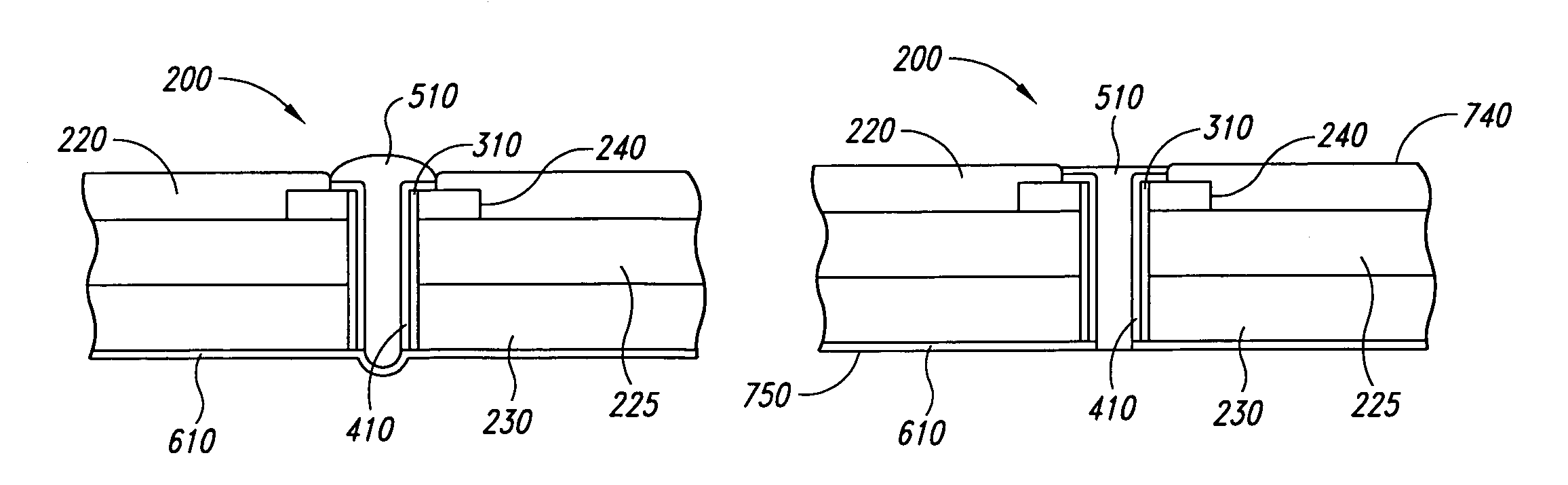
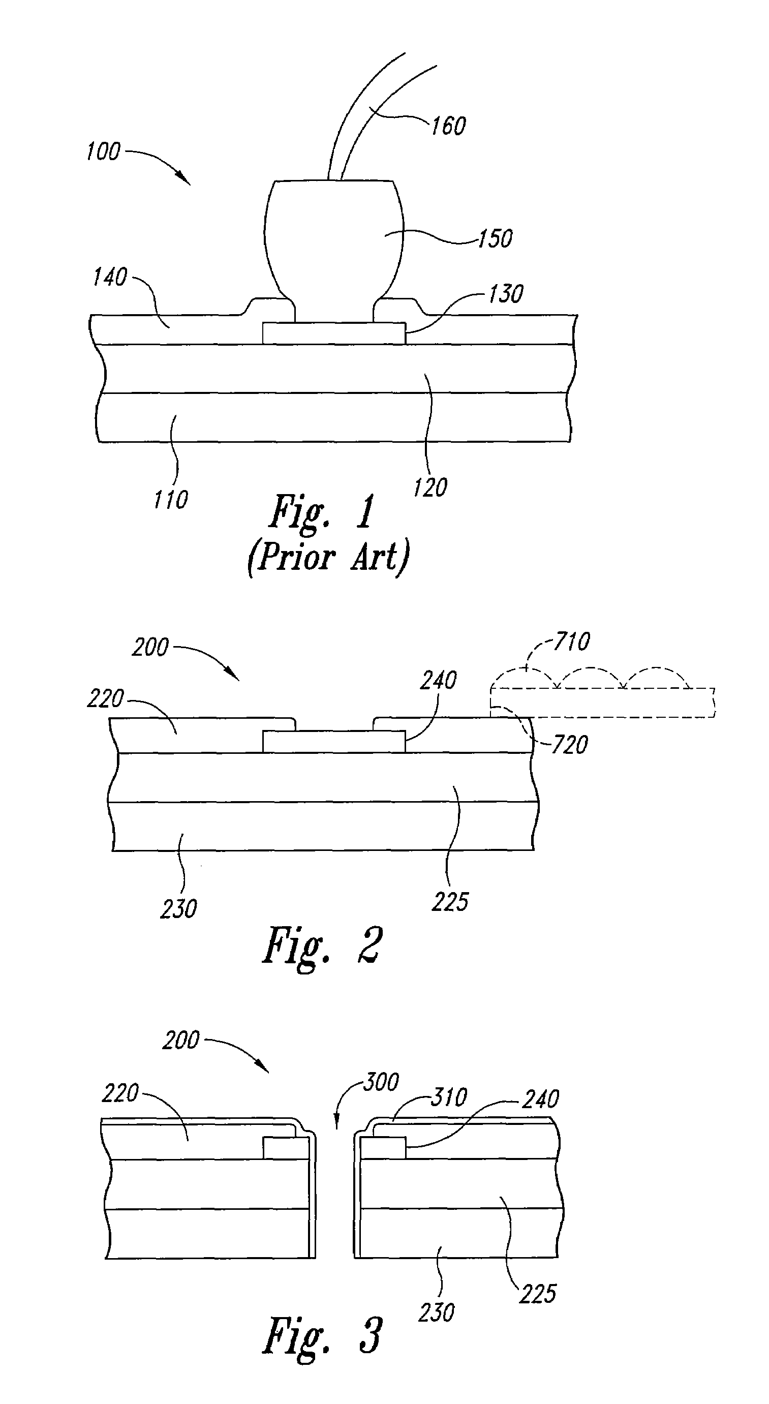
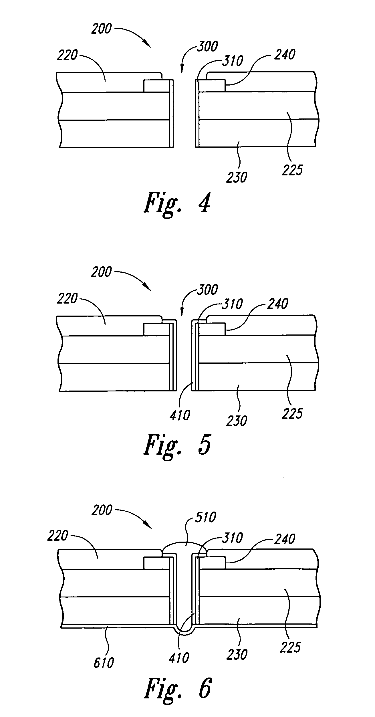
[0042]FIG. 2 depicts a portion of a semiconductor wafer 200 at a stage of a process for manufacturing a through-wafer interconnect for an integrated circuit device. A bond pad 240 is depicted as being formed over a silicon (Si) substrate 230 and within a passivation layer 220 or layers. Beneath the passivation layer 220 is a borophosphosilicate glass (BPSG) layer 225. The bond pad 240 is depicted as being a monolithic structure, however, the bond...


PUM


Abstract

A through-wafer interconnect for imager, memory and other integrated circuit applications is disclosed, thereby eliminating the need for wire bonding, making devices incorporating such interconnects stackable and enabling wafer level packaging for imager devices. Further, a smaller and more reliable die package is achieved and circuit parasitics (e.g., L and R) are reduced due to the reduced signal path lengths.

Description

FIELD OF THE INVENTION[0001]The present invention relates generally to imager and memory wafers, and more particularly to through-wafer interconnects and blind vias for imager and memory devices.BACKGROUND OF THE INVENTION[0002]As depicted in FIG. 1, a conventional bond pad structure 100 is built on a silicon substrate 110 covered by an oxide layer 120. The bond pad 130 is embedded within a passivation layer 140. A conductive gold wire (160) ball (150) bond is formed and attached on a central upper surface of the bond pad 130.[0003]A disadvantage of direct bond pad connection on the top side of the die, as depicted in FIG. 1, includes the fact that they sometimes require a wire bond 160 to be electrically connected to a lead frame or other structure for final die packaging. Another method that involves flip chip packaging at the wafer level involves a re-distribution layer (RDL) that allows the bond pad pitch to be routed to a more useable pitch in order to attach a solder ball dire...

Claims


Application Information

Patent Timeline
Patent Type & Authority Patents(United States)
IPC IPC(8): H01L21/441
CPCH01L21/6835H01L23/481H01L21/76898H01L21/76877H01L2224/48463H01L24/45H01L27/14634H01L27/14636H01L2221/6834H01L2224/16H01L2224/45144H01L2924/01014H01L2924/01029H01L2924/0105H01L2924/01078H01L2924/01079H01L2924/04941H01L2924/14H01L2924/00014H01L2924/10253H01L2924/01013H01L2924/01028H01L2924/00H01L2924/12042H01L2224/05567H01L2224/05573H01L2224/02166H01L2224/0554H01L24/11H01L24/13H01L2224/06181H01L24/05H01L24/03H01L2224/13025H01L2224/05599H01L2224/0555H01L2224/0556
Inventor AKRAM, SALMANWATKINS, CHARLESHIATT, MARKHEMBREE, DAVIDWARK, JAMESFARNWORTH, WARRENTUTTLE, MARKRIGG, SIDNEYOLIVER, STEVENKIRBY, KYLEWOOD, ALANVELICKY, LU
Owner ROUND ROCK RES LLC
Why Eureka
Try Eureka