Semiconductor Device

Inactive Publication Date: 2009-04-09
ROHM CO LTD
View PDF12 Cites 38 Cited by
  • Summary
  • Abstract
  • Description
  • Claims
  • Application Information

AI Technical Summary

Benefits of technology

[0029]The semiconductor device of the present invention can reduce a plane area by arranging the two output units configured to output different phases on the different planes intersecting with each other.
[0030]Moreover, according to the present invention, the second frequency for switching on and off the second switching device is higher than the first frequency for switching on and off the first switching device. Specificall

Problems solved by technology

However, the IPM disclosed in Patent Document 1 has a problem of an increased plane area since the power devices are provid

Method used


Image

  • Semiconductor Device
  • Semiconductor Device
  • Semiconductor Device

Examples


first embodiment

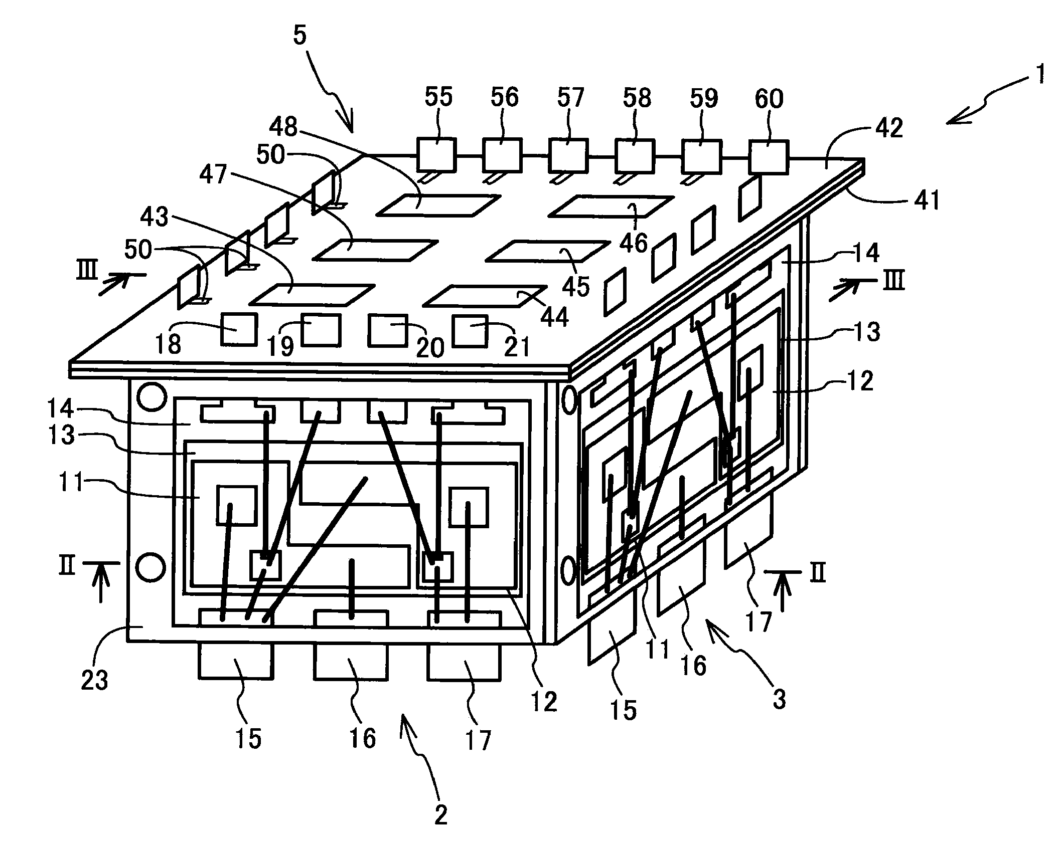
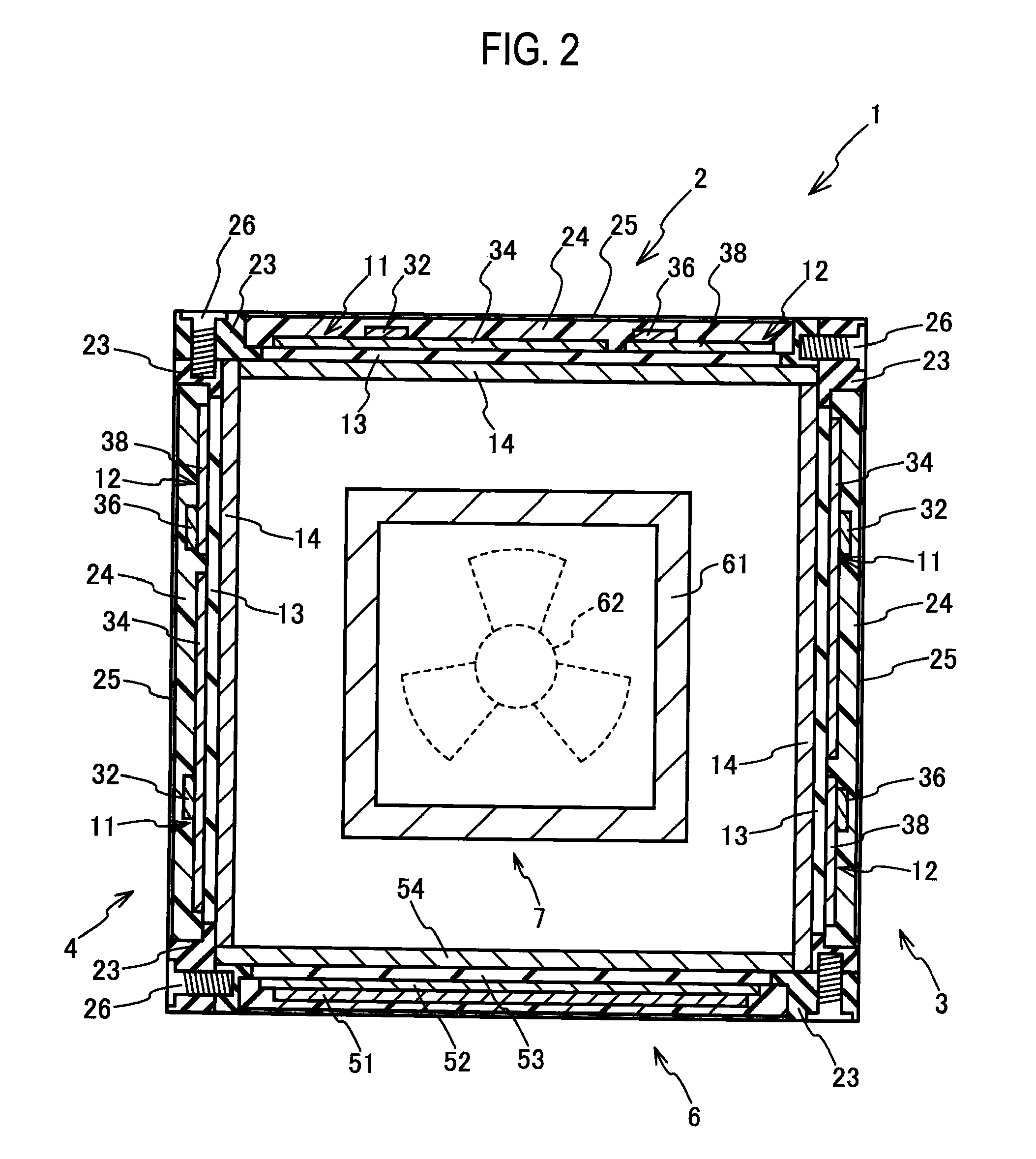
[0057]With reference to the drawings, description will be given of a first embodiment in which the present invention is applied to a three-phase intelligent power module (hereinafter referred to as an IPM). FIG. 1 is an overall perspective view of the IPM according to the first embodiment. FIG. 2 is a cross-sectional view along the line II-II in FIG. 1. FIG. 3 is a cross-sectional view along the line III-III in FIG. 1. FIG. 4 is a plan view of a U-phase output unit. FIG. 5 is a cross-sectional view along the line V-V in FIG. 4. FIG. 6 is a perspective view showing a switching device. FIG. 7 is a perspective view showing a diode. FIG. 8 is a schematic circuit diagram of the IPM.

[0058]As shown in FIGS. 1 to 3, an IPM 1 according to the first embodiment includes a U-phase output unit 2, a V-phase output unit 3, a W-phase output unit 4, a controller 5, a booster 6 and a cooler 7. The output units 2 to 4 configured to output different phases, the controller 5 and the booster 6 are dispos...

second embodiment

[0084]Next, description will be given of a second embodiment obtained by partially modifying the first embodiment described above. Note that the same constituent components as those of the first embodiment are denoted by the same reference numerals and description thereof will be omitted. FIG. 12 is a cross-sectional view equivalent to FIG. 2, showing an IPM according to the second embodiment.

[0085]As shown in FIG. 12, in each of a U-phase output unit 2A, a V-phase output unit 3A and a W-phase output unit 4A in an IPM 1A according to the second embodiment, a radiator plate 14 is disposed on the outside of a wiring board 13, and a high voltage unit 11 and a low voltage unit 12 are disposed on the inside of the wiring board 13. Moreover, also in a booster 6A, a radiator plate 54 is disposed on the outside of a wiring board 53, and a booster circuit unit 51 is disposed on the inside of the wiring board 53.

[0086]In the IPM 1A of the second embodiment, heat radiation properties can be fu...

third embodiment

[0087]Next, description will be given of a third embodiment obtained by partially modifying the first embodiment described above. Note that the same constituent components as those of the first embodiment are denoted by the same reference numerals and description thereof will be omitted. FIG. 13 is a cross-sectional view equivalent to FIG. 2, showing an IPM according to the third embodiment.

[0088]As in an IPM 1B shown in FIG. 13, a booster may be omitted and a controller 5B may be provided at a position of the booster. Specifically, a case 23B is attached to the position where the booster has been disposed, and a heat insulator 41 and a wiring board 42 having gate drives (not shown) provided therein are sequentially stacked on the outside of the case 23B.

[0089]In the IPM 1B according to the third embodiment, phase output units 2 to 4 and a controller 5A are disposed on respectively different sides of the rectangular parallelepiped. Thus, air permeability is improved. Consequently, c...


PUM


Abstract

A semiconductor device includes: a first output unit configured to output a first phase; a second output unit configured to output a second phase different from the first phase, the second output unit being disposed on a plane intersecting with a plane having the first output unit disposed thereon; and a controller configured to control the output units.

Description

CROSS REFERENCE TO RELATED APPLICATIONS AND INCORPORATION BY REFERENCE[0001]This application is based upon and claims the benefit of priority from prior Japanese Patent Application P2007-249491 filed on Sep. 26, 2007 and P2008-021890 filed on Jan. 31, 2008; the entire contents of which are incorporated by reference herein.BACKGROUND OF THE INVENTION[0002]1. Field of the Invention[0003]The present invention relates to a semiconductor device that is an intelligent power module including a power device and a control circuit.[0004]Moreover, the present invention relates to a semiconductor device including a plurality of switching devices to be switched on and off at different frequencies.[0005]2. Description of the Related Art[0006]There has heretofore been known an IPM that is a power module in which a power device including an IGBT and the like and a control circuit for controlling a gate and the like of the IGBT are integrally provided.[0007]Japanese Patent Application Publication No...

Claims


Application Information

Patent Timeline
IPC IPC(8): H05K7/20
CPCH02M7/003H05K7/1432H05K7/20918H01L2924/30107H01L2924/00H01L2224/49171H05K7/14324H05K7/14329
Inventor OTSUKA, TAKUKAZUOKUMURA, KEIJISAITO, MASAO
Owner ROHM CO LTD
Why Eureka
Try Eureka