Semiconductor manufacturing apparatus and substrate processing method

Inactive Publication Date: 2009-04-16
KOKUSA ELECTRIC CO LTD
View PDF15 Cites 59 Cited by
  • Summary
  • Abstract
  • Description
  • Claims
  • Application Information

AI Technical Summary

Benefits of technology

[0014]An object of the present invention is to provide a semiconductor manufacturing apparatus and a substrate processing method that can reduc

Problems solved by technology

However, although the desired average temperature deviation M is attained, there is a limitation on the thickness uniformity of a film formed on the substrate.
In a semiconductor manufacturing apparatus, because of various reasons such as heater installation errors causing an improper distance between a heater element and a furnace, installation errors of quartz members such as a so-called inner tube and an outer tube of the semiconductor manufacturing apparatus, and variations of temperature caused by a supporting post of a so-called boat, a temperature difference can occur along the circumference of a substrate inside a furnace.
However, in such a semiconductor manufacturing apparatus, the temperature difference along the circumference of the substrate is not reduced in the case where a temperature can be meas

Method used


Image

  • Semiconductor manufacturing apparatus and substrate processing method
  • Semiconductor manufacturing apparatus and substrate processing method
  • Semiconductor manufacturing apparatus and substrate processing method

Examples


first embodiment

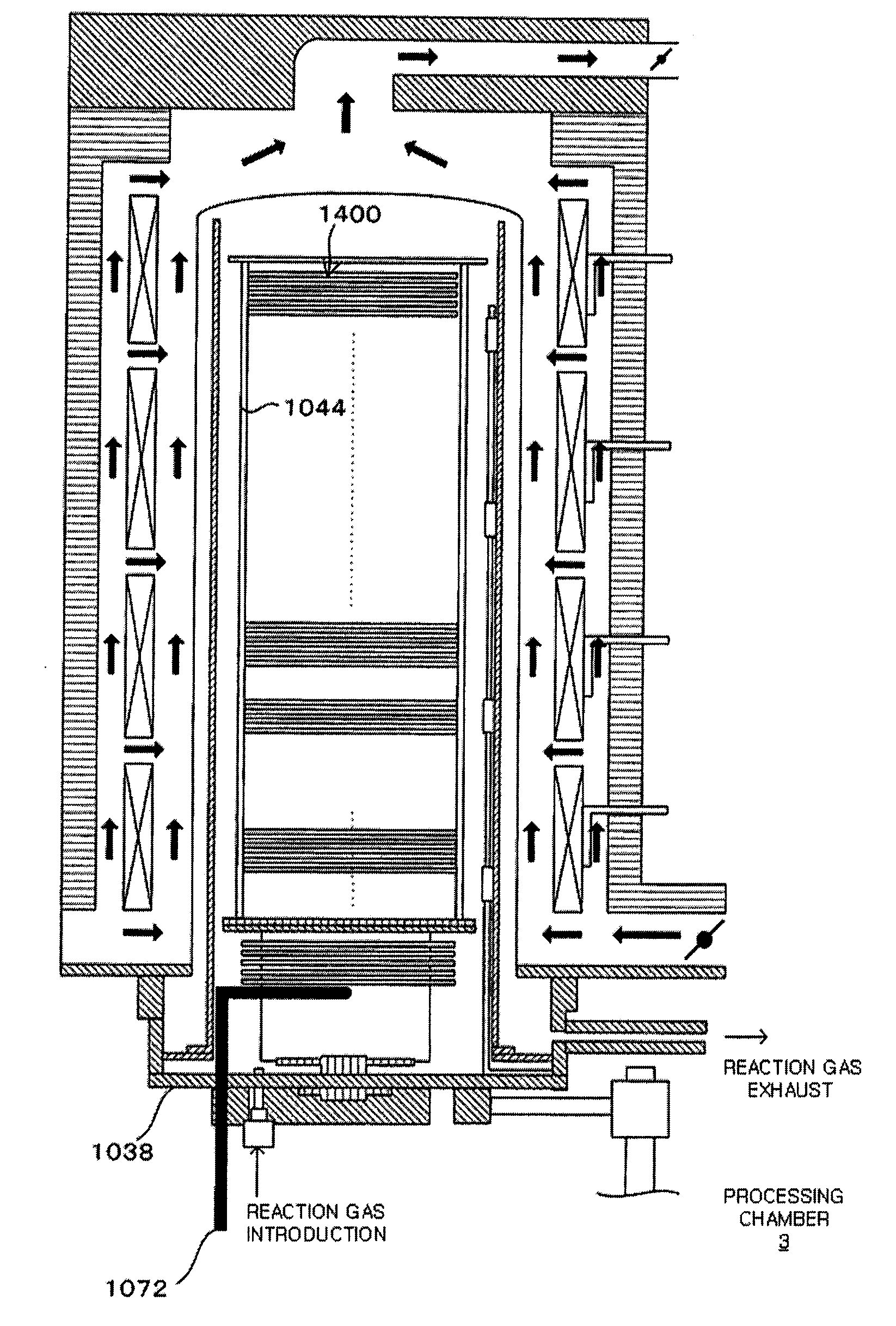
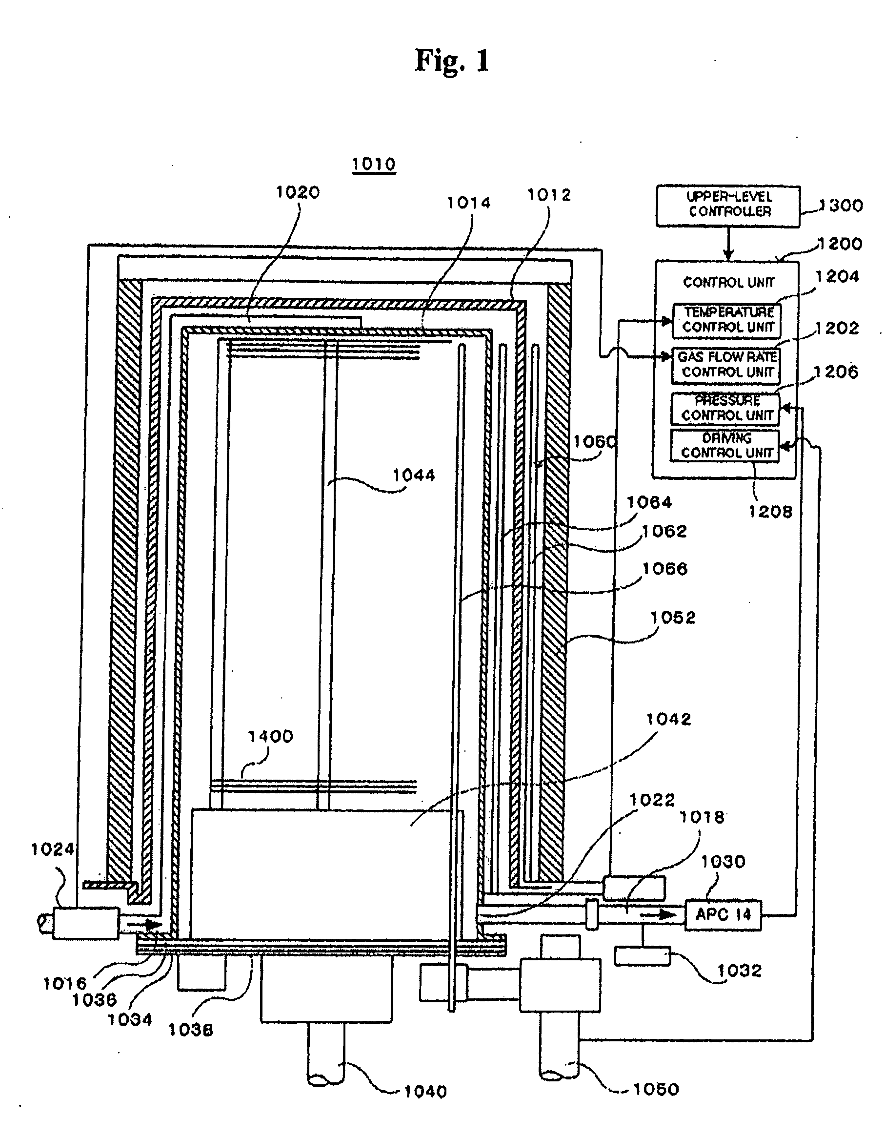
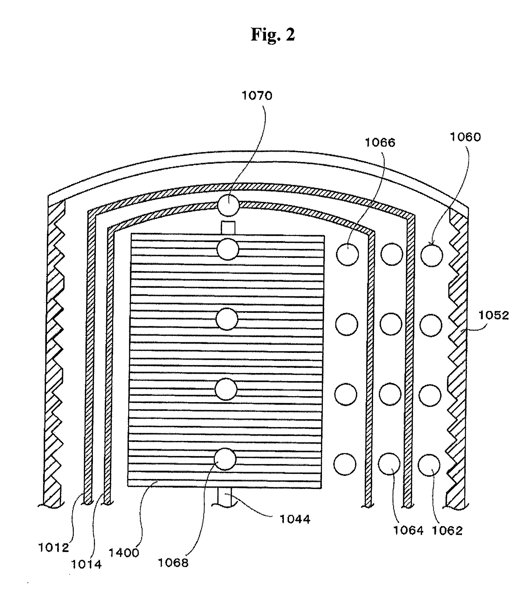
[0133]FIG. 11 illustrates a main part of a semiconductor manufacturing apparatus 1010 relevant to the present invention.

[0134]like in the first type to which the present invention is applied, the semiconductor manufacturing apparatus 1010 relevant to the first embodiment of the present invention includes a heater 1052 coaxially disposed at the outside of a reaction tube 1014, a first thermocouple 1062, second thermocouples 1064, and a third thermocouple 1066 (refer to FIG. 1).

[0135]As explained above, in the first type to which the present invention is applied, a second thermocouple 1064 is installed at the circumference of a wafer 1400. However, in the first embodiment, a plurality of second thermocouples 1064 are installed.

[0136]That is, as shown in FIG. 11, the semiconductor manufacturing apparatus 1010 relevant to the first embodiment includes a second main thermocouple 1064a (hereinafter, referred to as a inner main thermocouple), a second sub thermocouple 1064b (hereinafter, r...


PUM

PropertyMeasurementUnit
Temperatureaaaaaaaaaa
Pressureaaaaaaaaaa

Abstract

Provided are a semiconductor manufacturing apparatus and a substrate processing method that can reduce a temperature difference along the circumference of a substrate and continue substrate processing even when a temperature sensor becomes defective. The semiconductor manufacturing apparatus includes a reaction tube configured to process a wafer, a heater configured to heat the reaction tube, an exhaust pipe, a control unit configured to control a cooling gas exhaust device, the heater, and a pressure sensor that detects a pressure inside the exhaust pipe when cooling gas flows through the exhaust pipe. The control unit previously acquires an average value of second temperature detecting units that detect states of a peripheral part of a wafer, and a measure value of a first temperature detecting unit that detects a state of a center part of the wafer so as to control the heat and the cooling device based on the acquired values.

Description

CROSS-REFERENCE TO RELATED PATENT APPLICATION[0001]This U.S. non-provisional patent application claims priority under 35 U.S.C. § 119 of Japanese Patent Application Nos. 2007-231253, filed on Sep. 6, 2007, and 2008-170810, filed on Jun. 30, 2008, in the Japanese Patent Office, the entire contents of which are hereby incorporated by reference.BACKGROUND OF THE INVENTION[0002]1. Field of the Invention[0003]The present invention relates to a substrate processing method and a semiconductor manufacturing apparatus for processing a substrate such as a semiconductor wafer, and more particularly, to a substrate processing apparatus and a semiconductor manufacturing apparatus having a plurality of thermocouples used in heat treatment for measuring temperatures at positions near a substrate, the thermocouples being installed along the circumference of the substrate for using control values detected by the thermocouples in reducing a temperature difference along the circumference of the substr...

Claims


Application Information

Patent Timeline
IPC IPC(8): C23F1/00B05C11/00
CPCC23C16/4411C23C16/46C23C16/52H01L21/67248F27B17/0025H01L21/67109C30B25/16
Inventor SUGISHITA, MASASHIUENO, MASAAKIHAYASHIDA, AKIRA
Owner KOKUSA ELECTRIC CO LTD
Why Eureka
Try Eureka