System and method for suppression of wafer temperature drift in cold-wall cvd systems

Active Publication Date: 2006-03-16
NXP BV
View PDF46 Cites 42 Cited by
  • Summary
  • Abstract
  • Description
  • Claims
  • Application Information

AI Technical Summary

Benefits of technology

[0014] Yet another embodiment of the present invention is directed to a method to decrease temperature differences between wafers with different patterns or different thickness of the field oxide or nitride in epitaxial reactors. The method includes the steps of heating a wafer to a deposition temperature at a first pressure, registering

Problems solved by technology

As discussed more below, there is a problem caused by varying wafer temperature during non-selecti

Method used


Image

  • System and method for suppression of wafer temperature drift in cold-wall cvd systems
  • System and method for suppression of wafer temperature drift in cold-wall cvd systems
  • System and method for suppression of wafer temperature drift in cold-wall cvd systems

Examples


Example

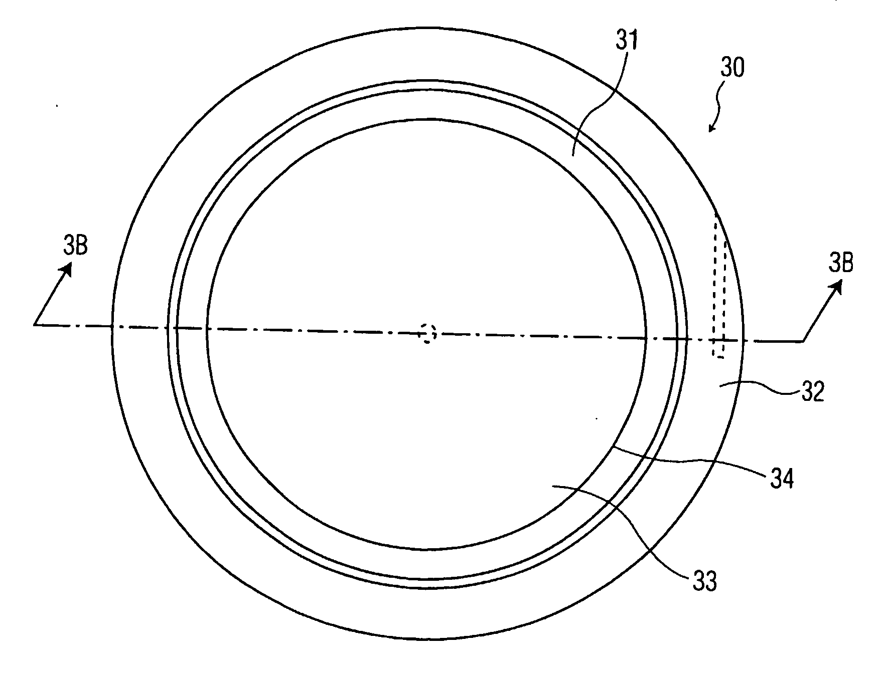
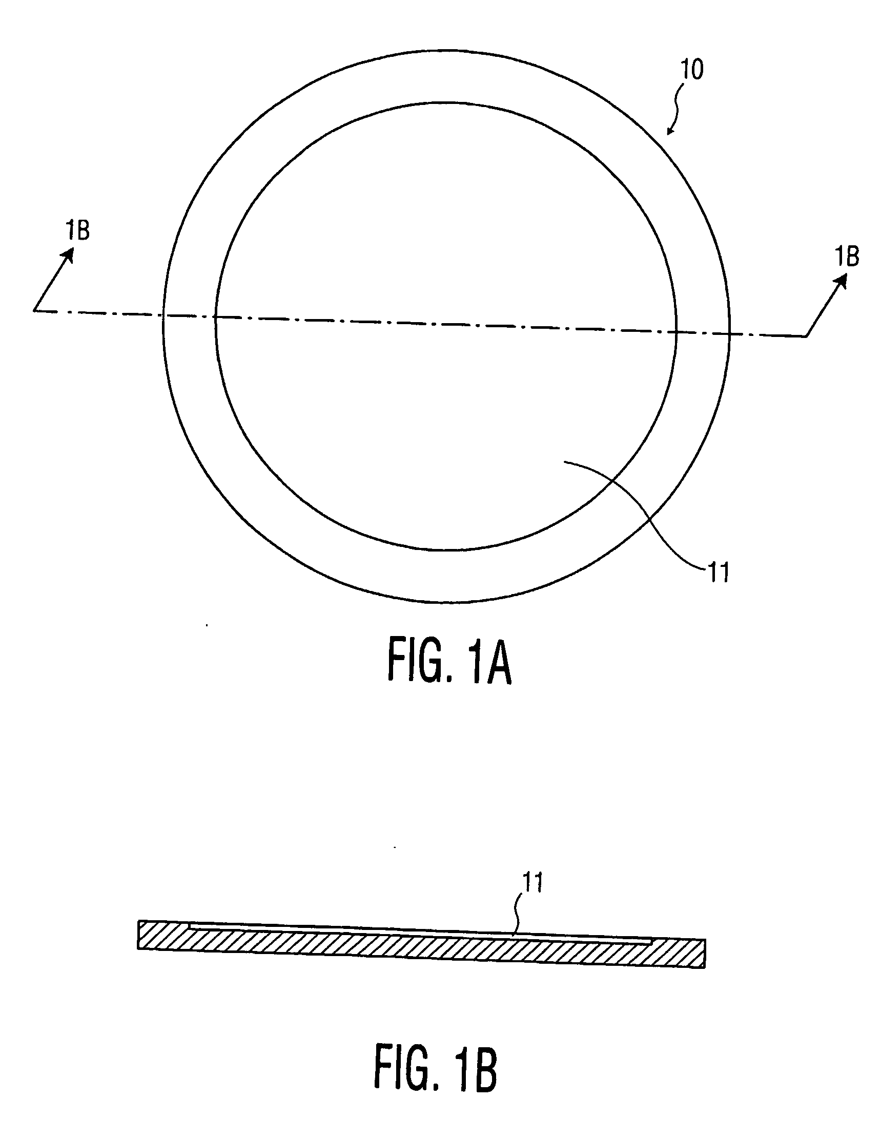
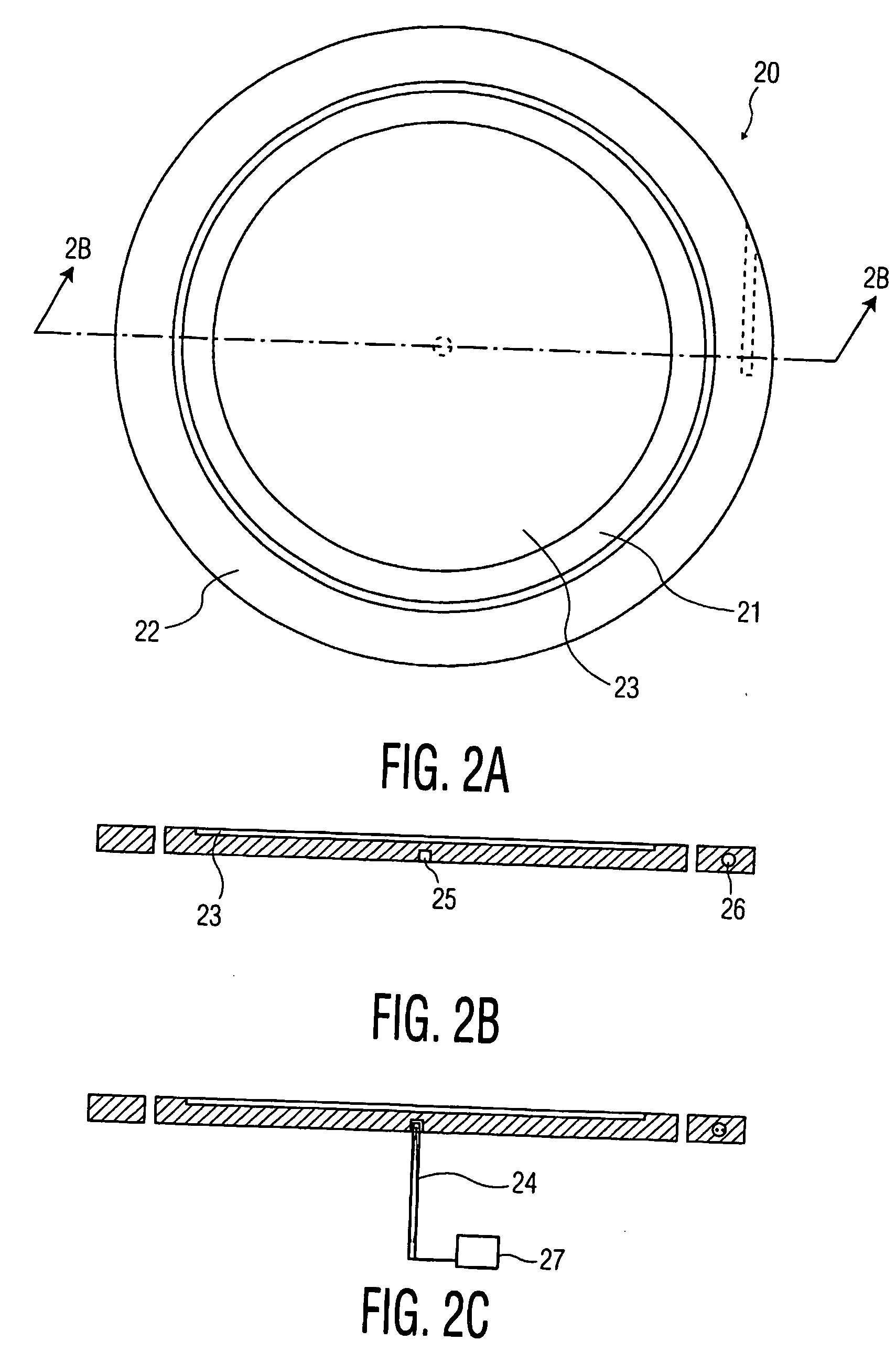
[0019] The assumption that a wafer is at approximately the same temperature as a susceptor is sufficiently close to reality at high temperatures. In this regard, high temperatures being defined as a temperature regime in which the growth rate is “transport limited.” The diffusion of fresh reactants to the surface of the wafer is the limiting factor and in this regime the growth rate is only moderately dependent on the temperature at high temperatures. Above 850-900° C. in case of silicon epitaxy, the systems described above may provide satisfactory results. However, at low temperatures this is no longer the case. There are two reasons why the susceptor temperature is an insufficient measure of the wafer temperature in the low-temperature range. In this regard, low-temperatures being defined as a temperature regime in which the growth rate is not “transport limited.”

[0020] First, it is noted that at low-temperatures, the growth rate of the wafer now is a strong function of the temper...


PUM

PropertyMeasurementUnit
Temperatureaaaaaaaaaa
Thicknessaaaaaaaaaa
Pressureaaaaaaaaaa

Abstract

An apparatus and corresponding method are disclosed that uses one or more optical fibers in a susceptor that monitor radiation emitted by the backside of the susceptor. The optical fibers are filtered and converted into an electrical signal. A control system is used to maintain a constant wafer temperature by keeping the electrical signal constant during the deposition cycle. This overcomes problems caused by varying wafer temperature during non-selective epitaxial and poly-silicon growth on patterned wafers at low temperatures and reduced pressure.

Description

FIELD OF THE INVENTION [0001] The present invention relates to the field of semiconductor wafer manufacturing. More particularly, the invention relates to a method and system for controlling and / or compensating for varying wafer temperature during non-selective epitaxial growth. BACKGROUND OF THE INVENTION [0002] Epitaxy is used in the semiconductor industry to grow a layer of semiconductor material on top of a single-crystalline semiconductor substrate in such a way that the crystal lattice is maintained. Common examples are the growth of an epitaxial silicon layer on top of a silicon substrate or the growth of a SiGe alloy layer on top of a silicon substrate. This can be done by chemical vapor deposition (CVD) in a proper environment. The wafer is heated to a suitable temperature and gases containing the required components are passed over the substrate, which usually is a silicon wafer. To avoid growth on the walls of the reactor vessel it is advantageous to heat just the wafer a...

Claims


Application Information

Patent Timeline
IPC IPC(8): H01L21/20C23C16/00H01L21/00
CPCH01L21/67248C30B25/16H01L21/20
Inventor DE BOER, WIEBE
Owner NXP BV
Why Eureka
Try Eureka