Link processing with high speed beam deflection

Active Publication Date: 2009-04-16
ELECTRO SCI IND INC
View PDF30 Cites 45 Cited by
  • Summary
  • Abstract
  • Description
  • Claims
  • Application Information

AI Technical Summary

Problems solved by technology

Recently, the use of new materials, such as aluminum, gold, and copper, coupled with the small geometry of these devices, have made the problem of link removal more difficult.
Thus, it can be increasingly difficult to irradiate a target struct

Method used


Image

  • Link processing with high speed beam deflection
  • Link processing with high speed beam deflection
  • Link processing with high speed beam deflection

Examples


Embodiment Construction

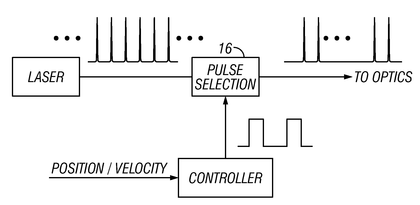
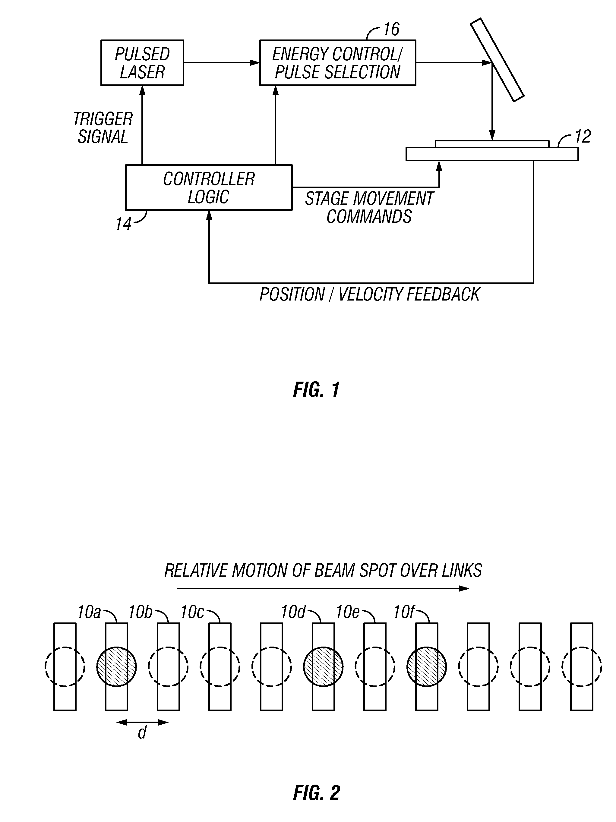
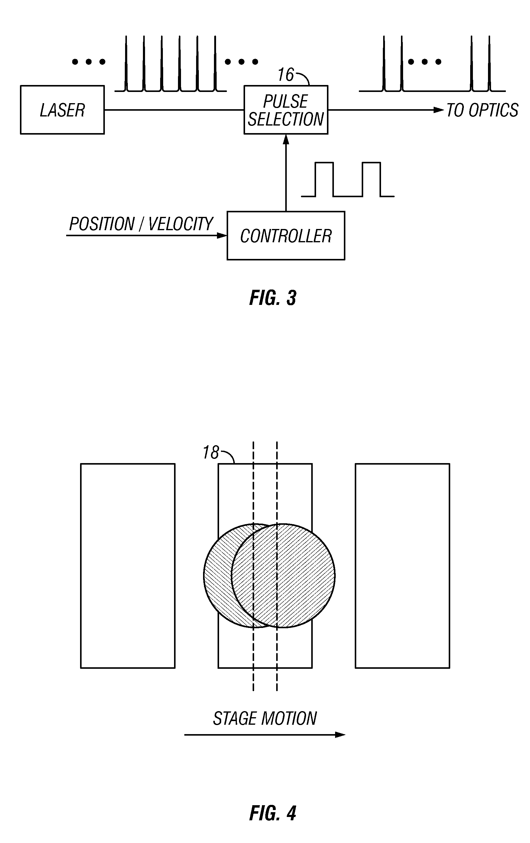
[0062]Methods and systems described herein relate to laser processing target structures of multi-material devices utilize multiple laser pulses. While this invention is well suited for improvements in processing closely spaced metal and non-metal links on semiconductor substrates, other types of multi-material devices may be laser processed with various benefits including, but not limited to increased process throughput, increased accuracy, reduced substrate damage, and reduced damage to adjacent devices.

[0063]General Aspects of Laser Processing of Target Microstructures

[0064]Many aspects of processing links on a multi-material device that may be used advantageously with this invention are described in sections [0115] to [0159], [0169] to [0175], and [0213] to [0225] of U.S. Patent Publication 2002 / 0167581, which is mentioned above.

[0065]A multi-material device may include a plurality of target structures positioned over a substrate. A pulsed laser beam, the beam having pre-determin...


PUM

PropertyMeasurementUnit
Electrical conductoraaaaaaaaaa
Erroraaaaaaaaaa
Velocityaaaaaaaaaa

Abstract

The present invention relates to the field of laser processing methods and systems, and specifically, to laser processing methods and systems for laser processing multi-material devices. Systems and methods may utilize high speed deflectors to improve processing energy window and/or improve processing speed. In some embodiments, a deflector is used for non-orthogonal scanning of beam spots. In some embodiment, a deflector is used to implement non-synchronous processing of target structures.

Description

CROSS REFERENCE TO RELATED APPLICATIONS[0001]This application claims priority under 35 U.S.C. Section 119(e) to Provisional Application No. 60 / 994,404, filed on Sep. 19, 2007, which application is incorporated by reference in its entirety.BACKGROUND OF THE INVENTION[0002]1. Field of the Invention[0003]The present invention relates to the field of laser processing methods and systems, and specifically, to laser processing methods and systems for laser processing multi-material devices.[0004]2. Description of the Related Art[0005]Lasers can be used in the processing of microstructures in memory and integrated circuit devices. For example, laser pulses can be used to ablate conductive links or link portions in a memory device, such as DRAMs in order to substitute working redundant memory cells for defective memory cells during memory manufacture.[0006]Recently, the use of new materials, such as aluminum, gold, and copper, coupled with the small geometry of these devices, have made the ...

Claims


Application Information

Patent Timeline
IPC IPC(8): B23K26/36
CPCB23K26/038Y10T29/49156B23K26/0635B23K26/0639B23K26/0648B23K26/0665B23K26/0807B23K26/0853B23K26/4005B23K26/4085B23K2201/40H01L21/76894H01L23/5258H01L27/10844B23K26/0869B23K26/365B23K26/06H01L2924/0002B23K26/064B23K26/082B23K26/0344B23K26/0624B23K26/40B23K26/361B23K2101/40B23K2103/16B23K2103/50H10B12/01H01L2924/00B23K26/08H01L21/768H01L21/822B23K26/0622
Inventor EHRMANN, JONATHAN S.GRIFFITHS, JOSEPH J.CORDINGLEY, JAMES J.SVETKOFF, DONALD J.JOHNSON, SHEPARD D.PLOTKIN, MICHAEL
Owner ELECTRO SCI IND INC
Why Eureka
Try Eureka