

Inverter control circuit and control method thereof
- Summary
- Abstract
- Description
- Claims
- Application Information
AI Technical Summary
Benefits of technology
Problems solved by technology
Method used
Image

Examples
embodiment 1
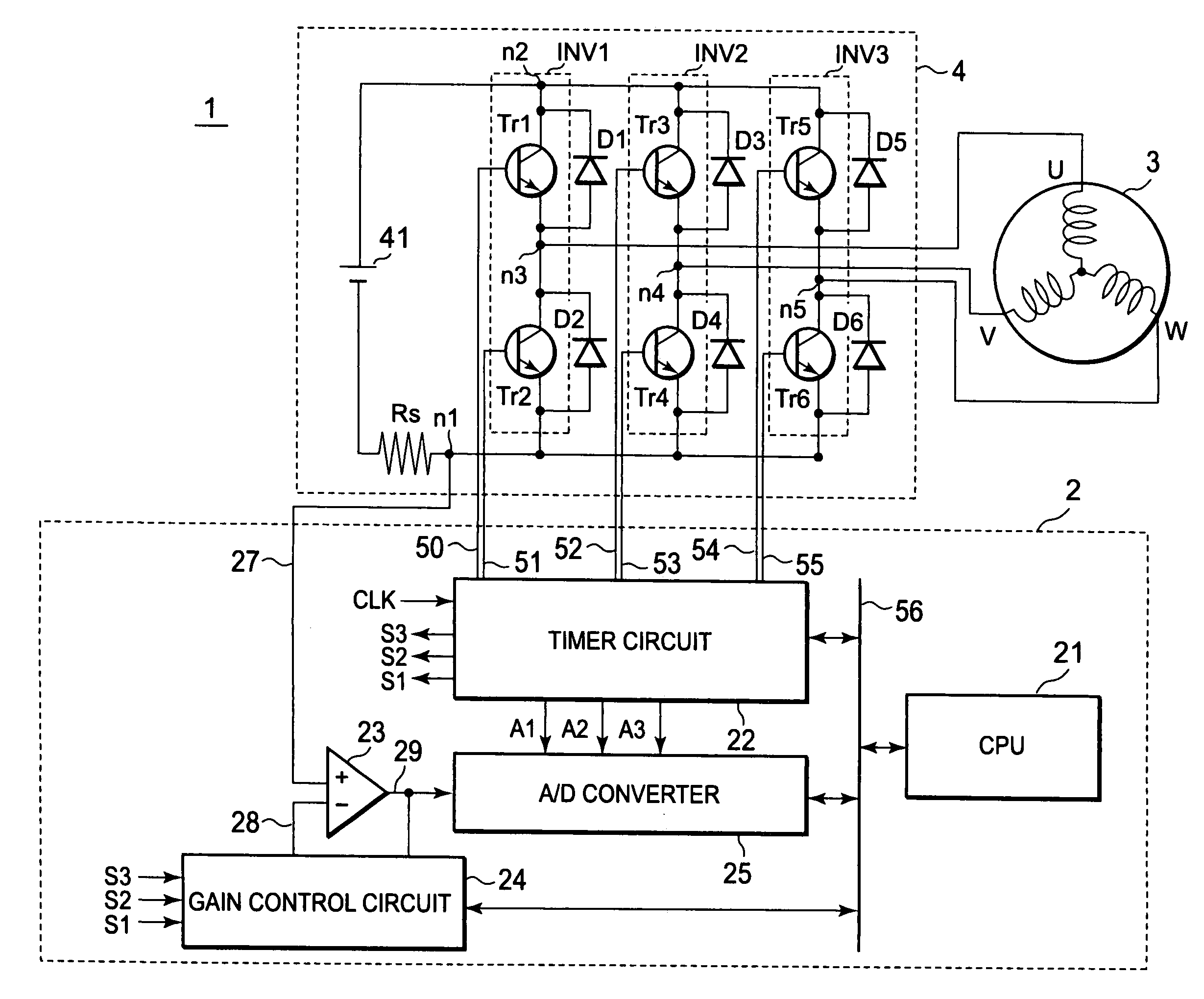
[0019]FIG. 1 is a block diagram showing a configuration example of a motor control system including an inverter control circuit of this embodiment. For a motor, an example in which a 3-phase motor is driven is illustrated. A current flown into a motor coil 3 is controlled by an inverter circuit 4. The inverter circuit 4 includes a plurality of switch devices Tr1 to Tr6, and adjusts a current supplied to a motor by turning ON / OFF the switch devices Tr1 to Tr6, in response to a 6-phase PWM signal inputted from a microcomputer 2. In FIG. 1, for a motor which is a control target, a motor coil 3 is only depicted. In the following description of this embodiment, the motor coil 3 with three coil phases and an inverter INV of the inverter circuit 4 with three phases are described as an example, but the number of phases for coils and that of an inverter of the invention are not limited to those described above for the examples.
[0020]The microcomputer 2 outputs, to the inverter circuit 4, a s...
embodiment 2
[0077]In Embodiment 1 of the invention, on the measurement of the analog signal 27 from the inverter circuit 4, during one period (the period from t0 to t13) in which the up / down counter 211 counts up from 0 to the maximum value M and, thereafter, counts down from M to 0, V0, V1, and V2 are measured only while counting up. However, described below is an example in which the voltage of the analog signal 27 is measured during both the count-up period and the count-down period in the one period. Thus, it becomes possible to measure a change of the voltage level with a higher degree of accuracy than that in Embodiment 1 of the invention, so that a feedback control can be performed.
[0078]In Embodiment 2 of the invention, the gain switching signals S1, S2, and S3 described in Embodiment 1 are respectively outputted twice in the one period of the up / down counter 211. Further, the A / D trigger signals A1, A2, and A3 of the A / D converter 25 are similarly outputted twice in the one period, and...
embodiment 3
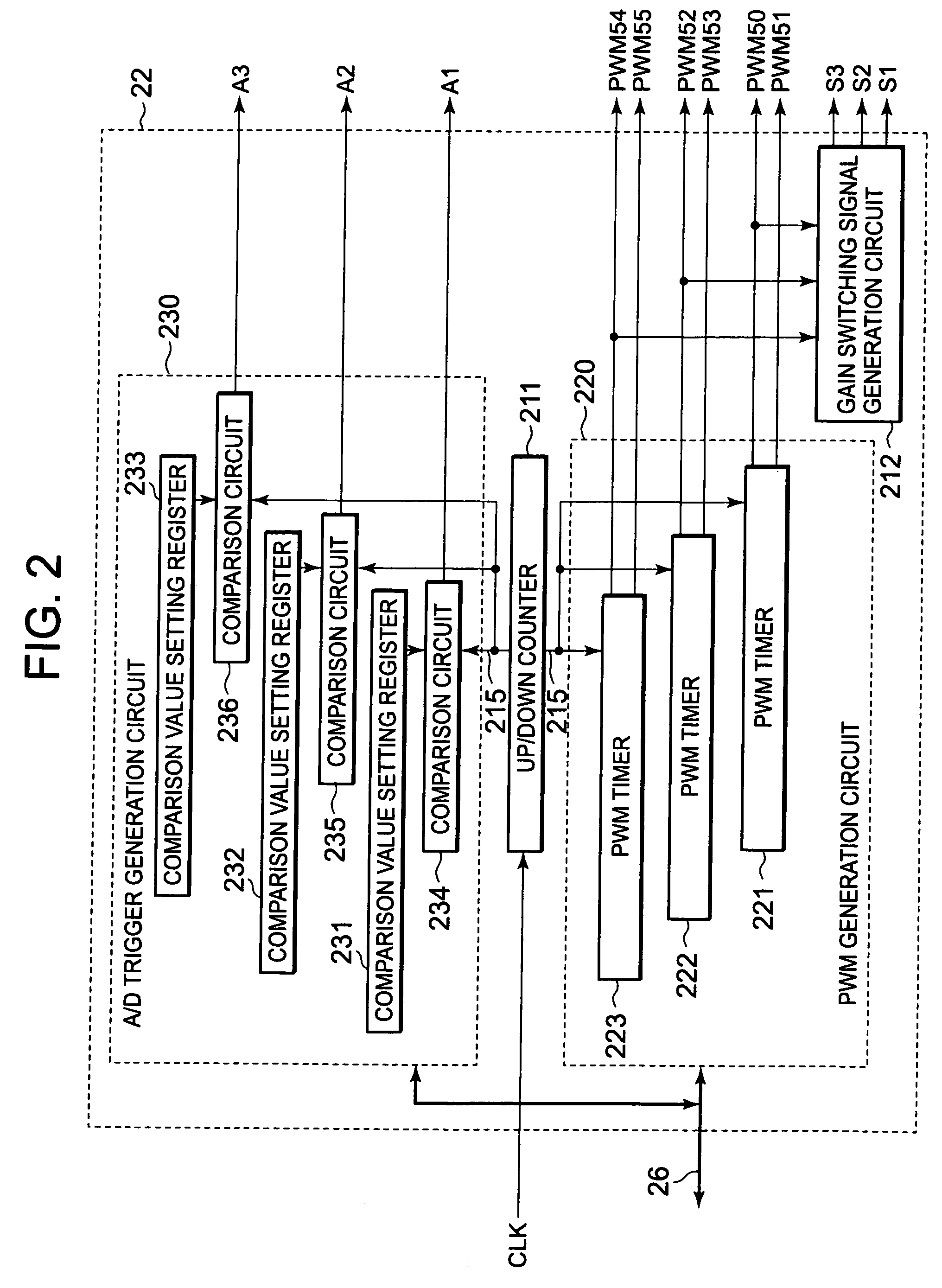
[0084]An A / D trigger generation circuit 250 is shown as another configuration example different from that of the A / D trigger generation circuit 230 in Embodiments 1 and 2 of the invention. Other configurations than that of the A / D trigger generation circuit 250 are the same as those of Embodiment 1. The timers 251, 252, and 253 each include a counter which counts up in response to a clock CLK inputted therein, a comparison value register, and a comparison circuit which compares the counter and the comparison value register, in which comparison value register a predetermined value is set through a bus 27 by the CPU 21, and generates a pulse signal when the set value and a count value match (the counter, the comparison value register, and the comparison circuit in each timer are not shown).
[0085]Connected to a gain switching signal S1, and once the counter in the timer 251 is cleared in response to the pulse input of S1, the timer 251 counts up from 0; and when the comparison circuit ...
PUM
 Abstract
Description
Claims
Application Information