Electron blocking layers for electronic devices

US20090101965A1Active Publication Date: 2009-04-23SANDISK TECH LLC
17 Cites 25 Cited by

Patent Information

Authority / Receiving Office
US · United States
Patent Type
Applications(United States)
Current Assignee / Owner
Publication Date
2009-04-23

Smart Images

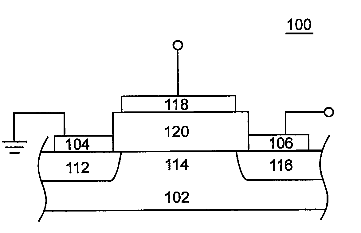
  • Figure 1
    Figure 1
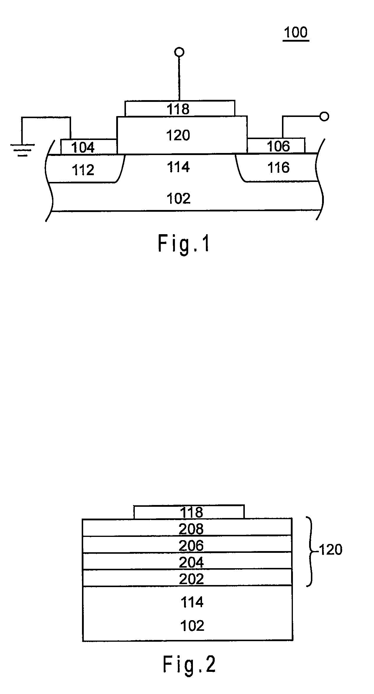
  • Figure 2
    Figure 2
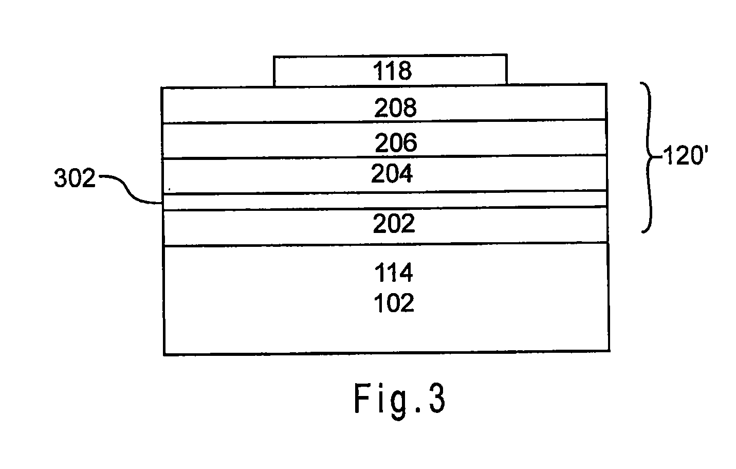
  • Figure 3
    Figure 3
Patent Text Reader

Abstract

Methods and apparatuses for electronic devices such as non-volatile memory devices are described. The memory devices include a multi-layer control dielectric, such as a double or triple layer. The multi-layer control dielectric includes a combination of high-k dielectric materials such as aluminum oxide, hafnium oxide, and / or hybrid films of hafnium aluminum oxide. The multi-layer control dielectric provides enhanced characteristics, including increased charge retention, enhanced memory program / erase window, improved reliability and stability, with feasibility for single or multi state (e.g., two, three or four bit) operation.
Need to check novelty before this filing date? Find Prior Art

Description

CROSS-REFERENCE TO RELATED APPLICATIONS

[0001] The present patent document is a continuation-in-part of PCT International Patent Application No. PCT / US2007 / 087167, which was filed on Dec. 12, 2007, and which claims priority to U.S. Provisional Patent Application Ser. No. 60 / 931,488, which was filed on May 23, 2007, and to U.S. patent application Ser. No. 11 / 743,085, filed on May 1, 2007, which is a continuation-in-part of U.S. patent application Ser. No. 11 / 688,087, filed on Mar. 19, 2007, which is a continuation-in-part of U.S. patent application Ser. No. 11 / 641,956, filed on Dec. 20, 2006, the entire contents of which are hereby incorporated by reference.TECHNICAL FIELD

[0002] The present disclosure relates to memory devices, and more particularly, to flash memory devices.BACKGROUND OF THE INVENTION

[0003] Non-volatile memory devices, such as flash memory devices, are memory devices that can store information even when not powered. A flash memory device stores information in a charge st...

Examples

Embodiment Construction

Introduction

[0037]It should be appreciated that the particular implementations shown and described herein are exemplary and are not intended to otherwise limit the scope of the present invention in any way. Indeed, for the sake of brevity, conventional electronics, manufacturing, semiconductor devices, and other functional aspects of the systems (and components of the individual operating components of the systems) may not be described in detail herein.

[0038]It should be understood that the spatial descriptions (e.g., “above,”“below,”“up,”“down,”“top,”“bottom,” etc.) made herein are for purposes of illustration only, and that devices described herein can be spatially arranged in any orientation or manner.

[0039]The terms “adjacent,”“on,”“over,” and “overlying,” as used herein to describe the relationship of one layer to another layer, are intended to be interpreted broadly to include layers in direct contact with one another and layers spaced apart by one or more intervening layers. ...