Design structure for uniform triggering of multifinger semiconductor devices with tunable trigger voltage

a design structure and semiconductor technology, applied in semiconductor devices, semiconductor/solid-state device details, electrical devices, etc., can solve the problems of reducing the current capacity of the esd protection mosfet, requiring a large clamping voltage, and generally required multiple fingers

Active Publication Date: 2009-04-30
IBM CORP
View PDF20 Cites 17 Cited by
  • Summary
  • Abstract
  • Description
  • Claims
  • Application Information

AI Technical Summary

Benefits of technology

[0063]In one embodiment, the semiconductor device is a metal oxide semiconductor fiel

Problems solved by technology

However, the multiple fingers of the ESD protection MOSFET typically do not turn on simultaneously due to differences in circuit parameters among the multiple fingers.
However, multiple fingers are generally required to handle the large amount of current during an ESD event.
However, this approach requires a large area of semiconductor substrate for such drain ballasting resistors.
Furthermore, the addition of drain ballasting resistors adds large on-resistance in the circuit, effectively reducing

Method used


Image

  • Design structure for uniform triggering of multifinger semiconductor devices with tunable trigger voltage
  • Design structure for uniform triggering of multifinger semiconductor devices with tunable trigger voltage
  • Design structure for uniform triggering of multifinger semiconductor devices with tunable trigger voltage

Examples


Embodiment Construction

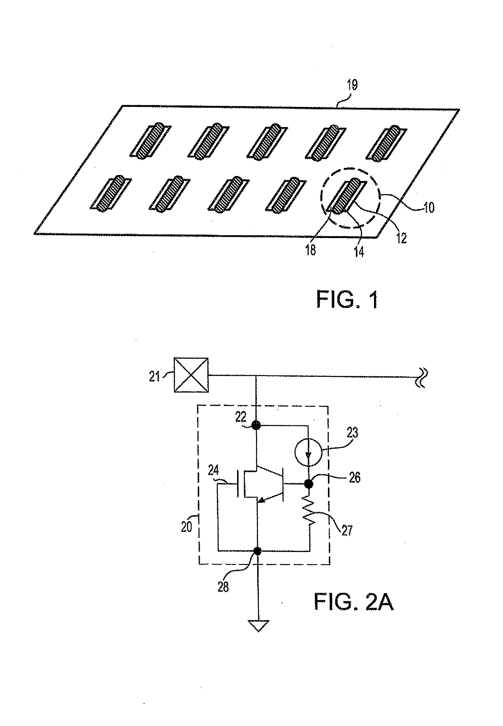
[0087]The present invention is herein described in detail with accompanying figures. While the present invention is described with specific examples, such as a 5 fingered gate-grounded NMOSFET (GGNMOSFET) and a 4×30 array finger configuration for a multi-fingered NMOSFET, these are only specific exemplary cases of implementation of the present invention and one of ordinary skill in the art would readily generalize the present invention to general multi-finger NMOSFETs, general multi-finger PMOSFETs, and multi-finger thyristors with any configurations for the multiple fingers.

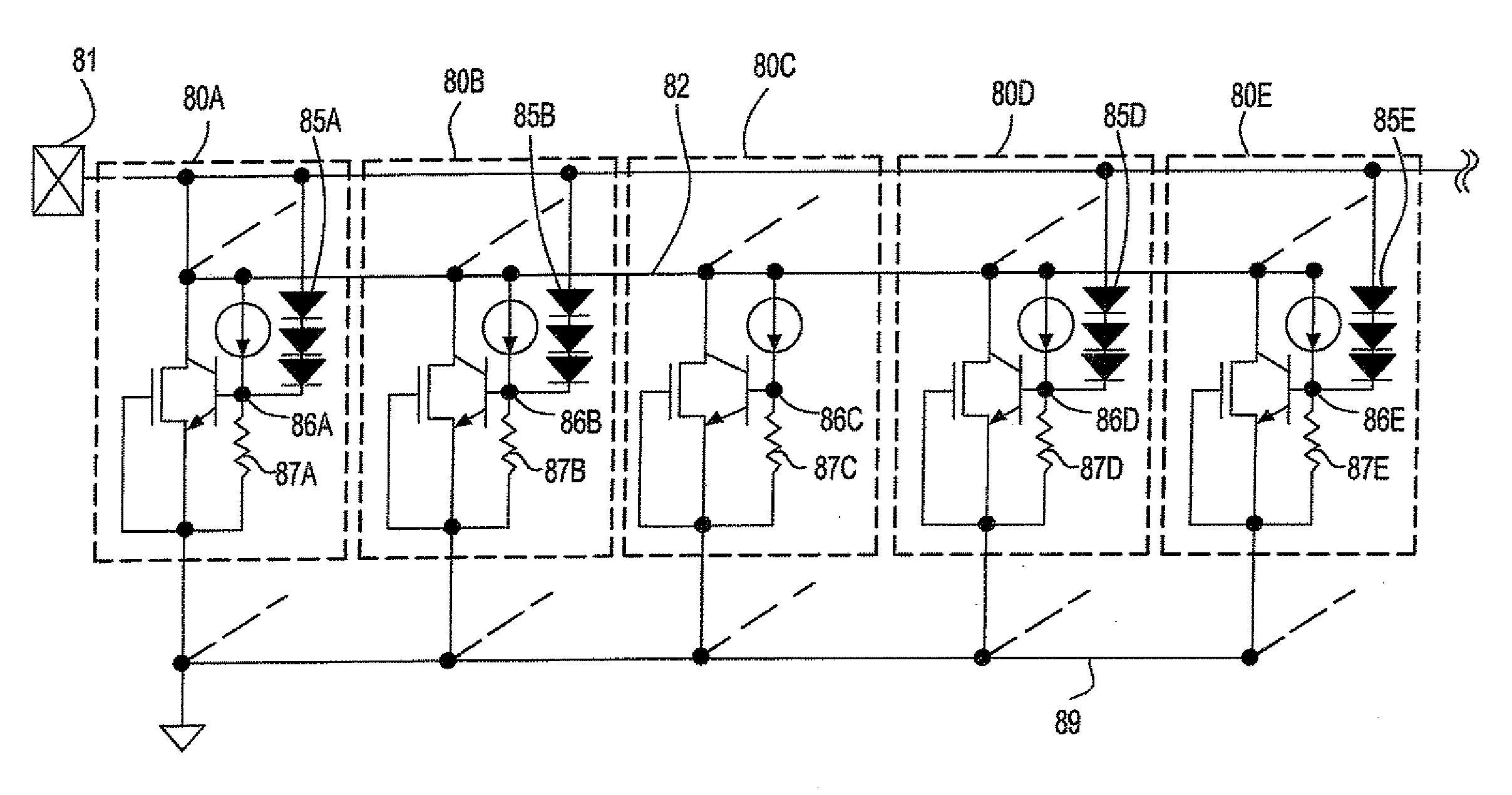
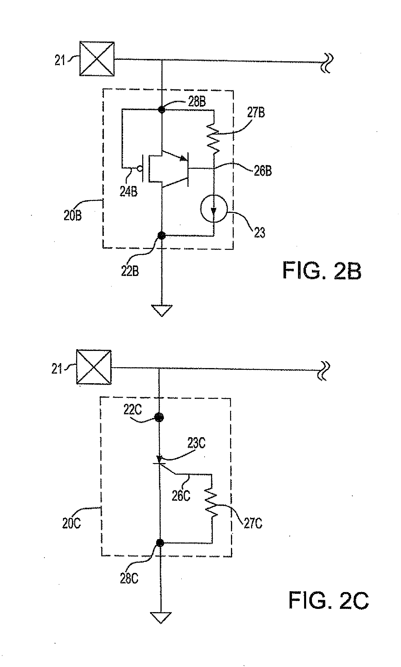
[0088]FIG. 4 shows a multi-finger NMOSFET ESD protection circuit according to the present invention. The circuit in FIG. 4 also has five fingers (40A-40E), each of which contains a parasitic bipolar transistor wherein the base (46A-46E) is the body of each finger, a parasitic injection source (43A-43E), and a parasitic resistor (47A-47E). The I / O pad 41 and the substrate ring contact 49 are identical to those in...


PUM


Abstract

A design structure for a circuit providing the same trigger voltage across the multiple fingers is provided, which comprises a data representing an external current injection source connected to individual fingers of a multi-finger semiconductor device. For example, the external injection current is supplied to the body of a MOSFET or the gate of a thyristor. The magnitude of the supplied current from each external current injection source is adjusted so that each finger has the same trigger voltage. The external current supply circuit may comprise diodes or an RC triggered MOSFET. The components of the external current supply circuit may be tuned to achieve a desired predetermined trigger voltage across all fingers of the multi-finger semiconductor device.

Description

RELATED APPLICATIONS[0001]The present application is related to co-pending U.S. patent application Ser. No. 11 / 692,481 filed on Mar. 28, 2007, which is incorporated herein by reference.FIELD OF THE INVENTION[0002]The present invention relates to semiconductor circuitry, and more particularly to a semiconductor circuit for uniform triggering of multifinger semiconductor devices, and a design structure on which the semiconductor circuit resides.BACKGROUND OF THE INVENTION[0003]In typical CMOS circuitry, semiconductor devices with multiple fingers are utilized and distributed over a wide area of a chip for various purposes. The multifinger semiconductor devices can also be considered multiple parallel devices with a common control component, such as a gate of a transistor or a thyristor. A typical example is an electrostatic discharge (ESD) protection circuit that requires placement of multiple fingers of a MOSFET in a parallel connection that is spread over a chip. In this case, distr...

Claims


Application Information

Patent Timeline
IPC IPC(8): H01L27/06
CPCH01L27/0259H01L27/0817H01L27/0727H01L27/0266
Inventor ABOU-KHALIL, MICHEL J.GAUTHIER, ROBERTLI, HONGMEILI, JUNJUNMITRA, SOUVICKPUTNAM, CHRISTOPHER S.
Owner IBM CORP
Why Eureka
Try Eureka