Design structure for CMOS differential rail-to-rail latch circuits

a latch circuit and design structure technology, applied in the field of metal oxide semiconductor circuits, can solve problems such as lack of synchronization between true output q and latch circuits

Inactive Publication Date: 2009-04-30
IBM CORP
View PDF11 Cites 32 Cited by
  • Summary
  • Abstract
  • Description
  • Claims
  • Application Information

AI Technical Summary

Benefits of technology

[0008]In accordance with another aspect of the invention, a design structure including a master-slave (“MS”) CMOS differential rail-to-rail flip-flop is provided which includes one or more instances of the CMOS differential rail-to-rail latch. In addition, a MS CMOS single-ended to differential flip-flop is provided which accepts a single-ended input signal and provides true and complementary output signals. A clock divider circuit can be provided which incorporates the MS CMOS single-ended to differential flip-flop.

Problems solved by technology

One problem with the flip-flop shown in FIG. 1A is lack of synchronism between the true output Q of the latch and the complementary output / Q.

Method used


Image

  • Design structure for CMOS differential rail-to-rail latch circuits
  • Design structure for CMOS differential rail-to-rail latch circuits
  • Design structure for CMOS differential rail-to-rail latch circuits

Examples


first embodiment

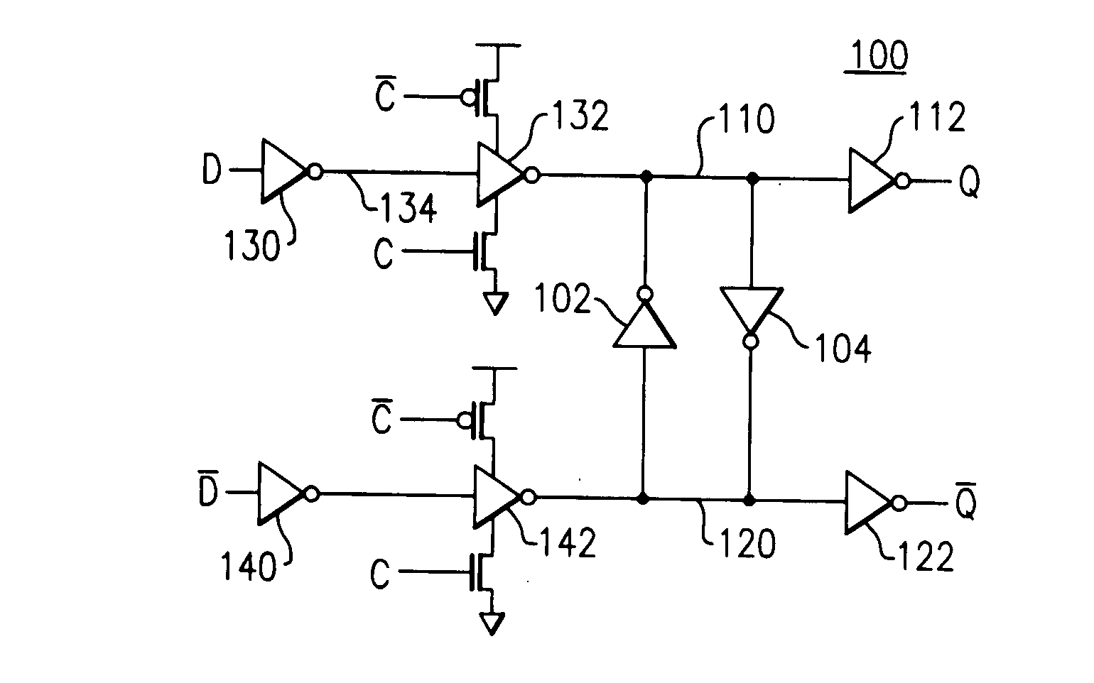
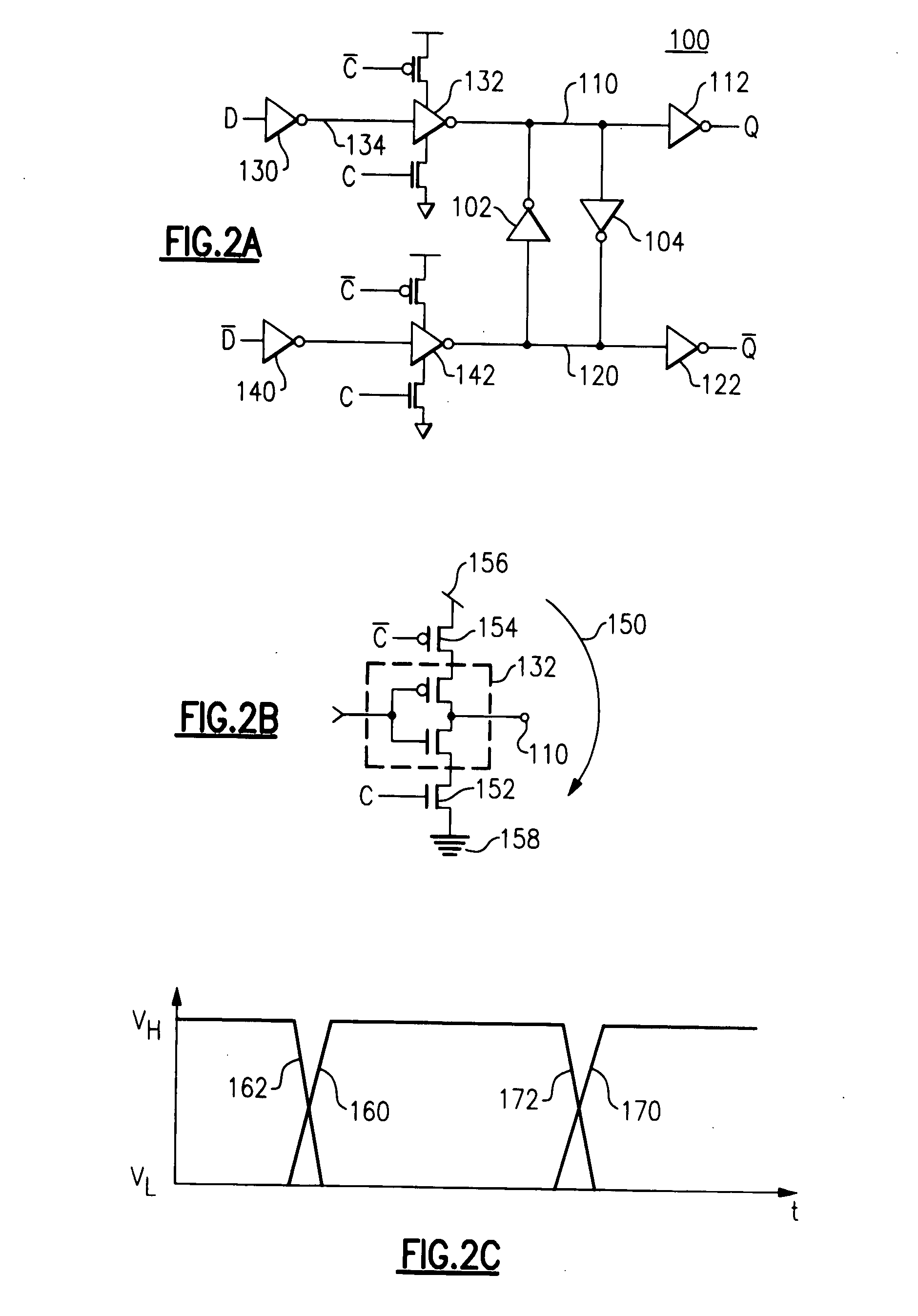
[0024]Commonly owned U.S. patent application Ser. No. 11 / 668,137 filed Jan. 29, 2007 to Joseph Natonio et al. entitled “CMOS Differential Rail-to-Rail Latch Circuits” is incorporated by reference herein. FIG. 2A illustrates a differential CMOS latch in accordance with the invention. As a CMOS circuit, the latch includes a pair of cross-coupled CMOS inverters 102, 104, which serve to maintain the logic states of a first node 110 and a second node 120 at rail-to-rail logic levels. With rail-to-rail logic levels, the high logic state is represented by a steady state voltage which usually is the same as a voltage level at which power is supplied to the source terminal of the pMOS device of each cross-coupled inverter in the latch. The low logic state usually is represented by ground, the voltage to which the source terminal of the nMOS device of each cross-coupled inverter of the latch is connected. By the action of the cross-coupled CMOS inverters 102, 104, when the first node 110 is a...

second embodiment

[0029]FIG. 3 illustrates an edge-triggered master-slave (“MS”) flip-flop 200 in accordance with the invention. The MS flip-flop includes two rail-to-rail differential CMOS latches 100A, 100B (FIGS. 2A-2C), arranged in series, such that the output signals / Q′ and Q′ of the first latch 100A are applied to the inputs of inverters 130B and 140B of the second latch 100B. As in the case of the differential CMOS latch 100, the output signals Q and / Q are differential signals, i.e., simultaneously swinging true and complementary signals with rail-to-rail signal levels.

[0030]In the MS flip-flop, inverters 132B and 142B of the second latch 100B are timed differently from the inverters 132A and 142A of the first latch 100A. In this case, the complementary clock signal / C is applied to the pMOS devices 154B, and the true clock signal C is applied to the nMOS devices 152B. On the other hand, in the first (master) latch 100A, the true clock signal C is applied to the pMOS devices 154A, and the co...


PUM


Abstract

A design structure including a CMOS rail-to-rail differential latch is provided in which a plurality of cross-coupled devices pull first and second nodes of the latch to opposite rail-to-rail voltages. Desirably, first and second output isolating elements have inputs coupled to the first and second nodes, the output isolating elements being operable to output versions of the opposite rail-to-rail voltages as a true and a complementary output of the latch. In this way, the true output has a rising edge occurring simultaneously with a falling edge of the complementary output. The complementary output has a rising edge occurring simultaneously with a falling edge of the true output. First and second input isolating elements of the latch have outputs coupled to the first and second nodes, the first and second input isolating elements being operable to apply versions of input signals to the first and second nodes.

Description

BACKGROUND OF THE INVENTION[0001]The present invention relates to complementary metal oxide semiconductor circuits, and more specifically to latch circuits, flip-flops and clock divider circuits.[0002]FIG. 1 is a block and schematic diagram illustrating the structure of a master-slave “D-type” flip-flop 10 in accordance with the prior art. Flip-flop 10 includes a first latch or “master” latch 12 formed by cross-coupled inverters 12A and 12B. Through an inverter 24, the master latch 12 is coupled to an input of a second latch or “slave” latch 14, the slave latch being formed by cross-coupled inverters 14A and 14B. The flip-flop 10 is clocked via a complementary clock signal pair (indicated as true clock signal C and complementary clock signal / C) applied to transmission gates 16, 18, 20, and 22. The flip-flop 10 accepts a single-ended data signal at the “D” input thereto. Once latched by the master latch 12 on the falling edge of the true clock signal C, the latched state of the data...

Claims


Application Information

Patent Timeline
Patent Type & Authority Applications(United States)
IPC IPC(8): H03K3/3562H03K21/00H03K3/00
CPCH03K3/35625
Inventor NATONIO, JOSEPHZIER, STEVEN J.
Owner IBM CORP
Why Eureka
Try Eureka