

High resistivity soi base wafer using thermally annealed substrate
- Summary
- Abstract
- Description
- Claims
- Application Information
AI Technical Summary
Benefits of technology
Problems solved by technology
Method used
Image

Examples
Embodiment Construction
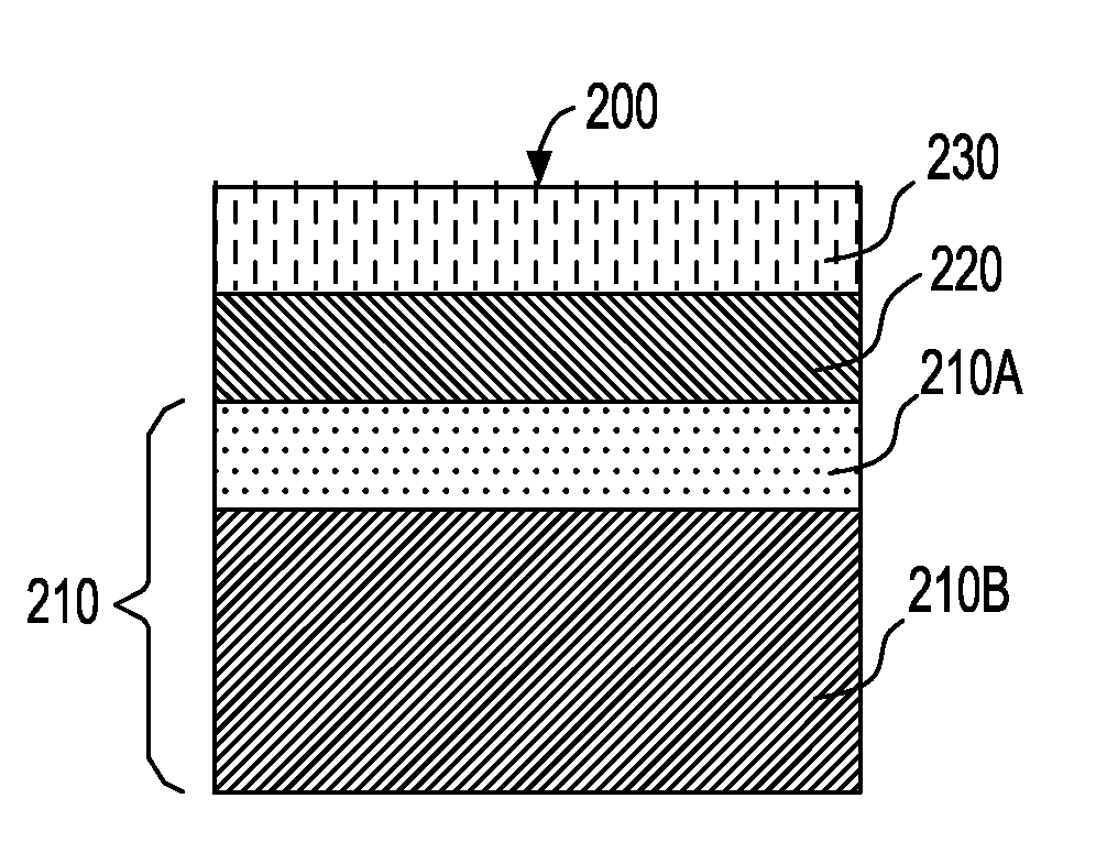
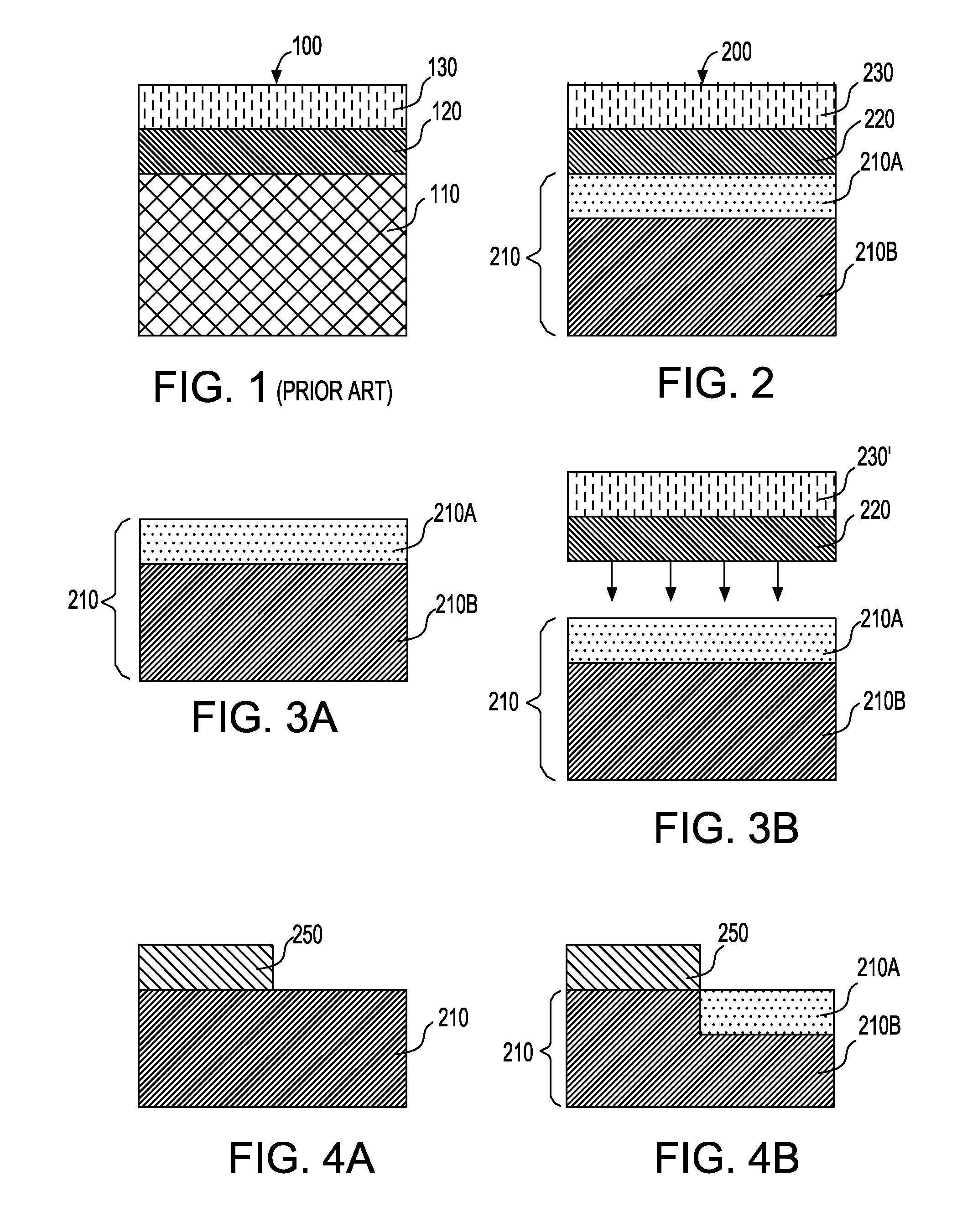
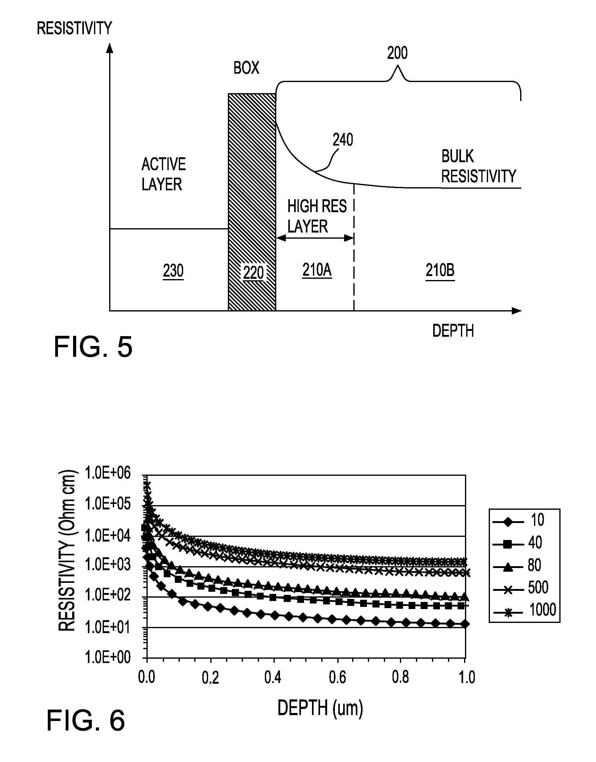
[0038]The present invention, which provides a method of fabricating an SOI wafer having an HR surface layer within the semiconductor base wafer as well as the SOI wafer that includes the HR surface layer within the semiconductor base layer, will now be described in more detail by referring to the drawings that accompany the present application. In the accompanying drawings, like and corresponding elements are referred to by like reference numerals. It is also noted that the drawings of the present invention representing the structures during the various processing steps of the present invention are provided for illustrative purposes and are thus not drawn to scale.
[0039]In the following description, numerous specific details are set forth, such as particular structures, components, materials, dimensions, processing steps and techniques, in order to provide a thorough understanding of the present invention. However, it will be appreciated by one of ordinary skill in the art that the ...
PUM
 Abstract
Description
Claims
Application Information