System and Method for Generating a Worst Case Current Waveform for Testing of Integrated Circuit Devices

a technology of integrated circuit devices and current waveforms, which is applied in the field of system and method for generating the worst case current waveform for the testing of integrated circuit devices, can solve the problems of power that the integrated circuit device dissipates, human error may be present in this determination, and considerable uncertainty in the estimation of guard bands, so as to reduce uncertainty, reduce uncertainty, and increase confiden

Inactive Publication Date: 2009-04-30
SONY COMPUTER ENTERTAINMENT INC +1
View PDF7 Cites 11 Cited by
  • Summary
  • Abstract
  • Description
  • Claims
  • Application Information

AI Technical Summary

Benefits of technology

[0007]In view of the above, it would be beneficial to have a system and method for determining a guard band for the minimum supply voltage of an integrated circuit device that significantly reduces the uncertainty in the determination of the guard band. One way in which to reduce uncertainty is to provide greater confidence in the determination of the worst case current waveform used to test the integrated circuit device. A system and method for generating a worst case current waveform for testing of integrated circuit devices is provided by the illustrative embodiments herein, as well as a system and method for the determination of a guard band, such that the uncertainty in generating the worst case current waveform and the guard band are reduced.

Problems solved by technology

For example, operating temperature, the process used to fabricate the integrated circuit device, and operating voltage all affect how the integrated circuit device will perform and the power that the integrated circuit device dissipates.
Since it is left to the human designer to determine this worst case current waveform, human error may be present in this determination.
Thus, there may be considerable uncertainty in the estimation of the guard band to apply to the empirically determined minimum supply voltage VminF, as well as the uncertainty in the determination of the worst case current waveform.
The worst case power workload is thus, a sequence of instructions that may be fed to the pipeline of the integrated circuit device that will cause the transistors in each of the stages of the pipeline to be activated, i.e. will cause a switching of the transistors and thus, an active power consumption.
This worst case power workload may be a combination of instructions and data that do not in fact provide any useful code sequence or data pattern, i.e. it would not generally be utilized during the lifetime of the integrated circuit device, but still provides a worst case approximation of the power consumption of the integrated circuit device.

Method used


Image

  • System and Method for Generating a Worst Case Current Waveform for Testing of Integrated Circuit Devices
  • System and Method for Generating a Worst Case Current Waveform for Testing of Integrated Circuit Devices
  • System and Method for Generating a Worst Case Current Waveform for Testing of Integrated Circuit Devices

Examples


Embodiment Construction

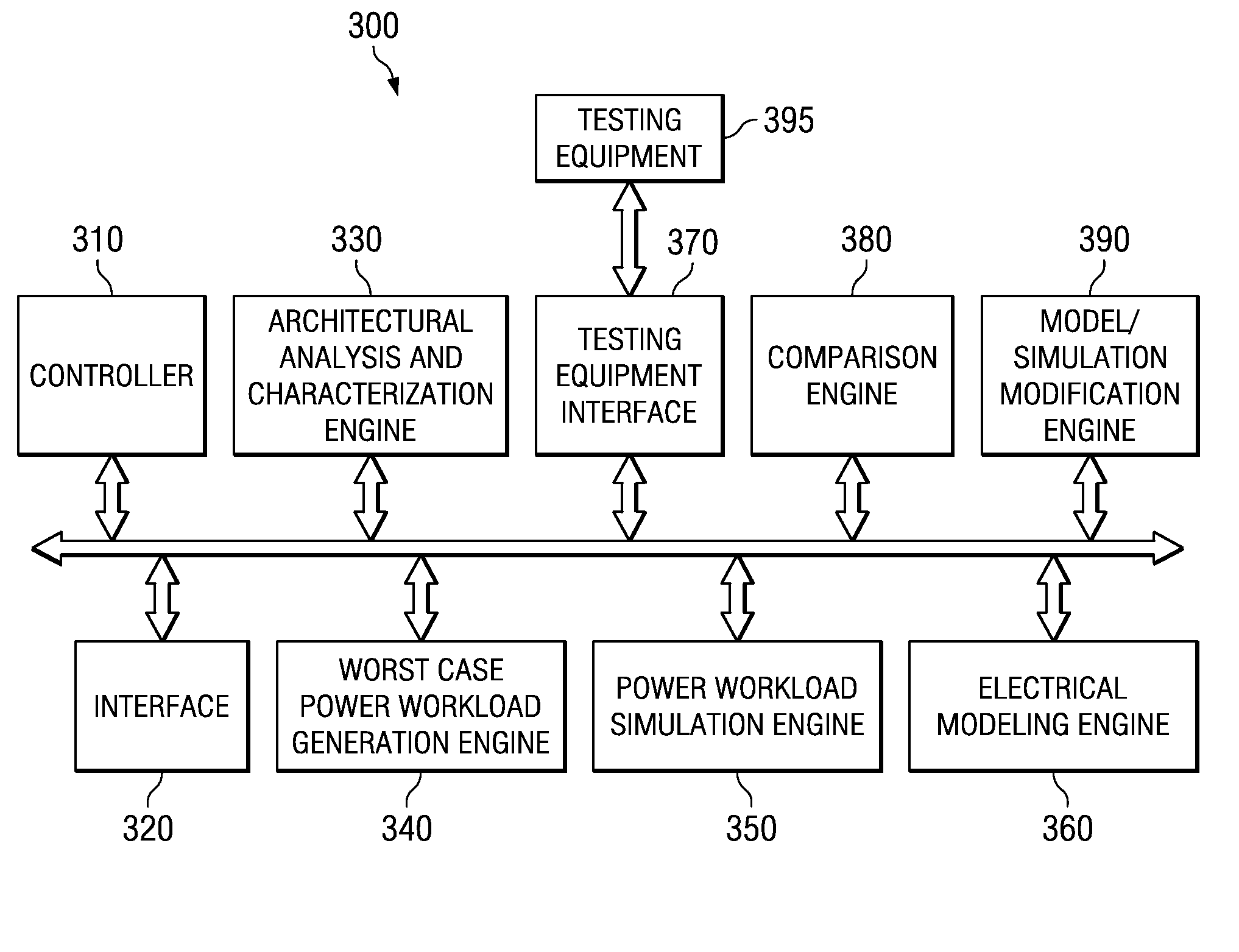
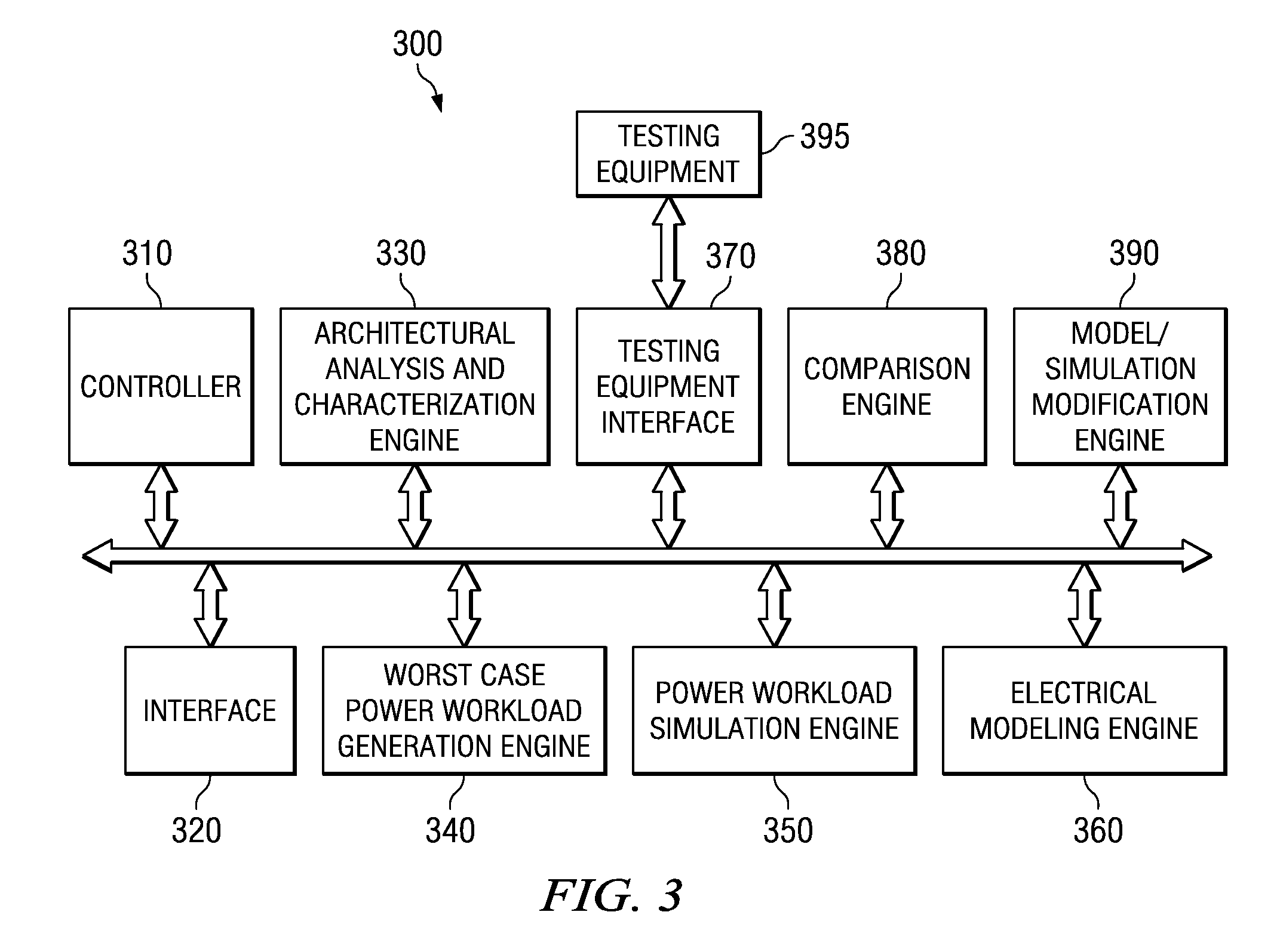
[0042]The illustrative embodiments provide a mechanism for determining worst case current waveform for testing an integrated circuit device, such as a processor, chip, package, or the like, in order to obtain a guard band for an operating voltage of an integrated circuit device, such as an integrated circuit chip. The worst case current waveform is determined through a combination of simulation and hardware measurement of the integrated circuit device in order to obtain a worst case current waveform that accurately represents the actual hardware processing of a worst case power workload.

[0043]Having obtained a worst case current waveform through operation of the illustrative embodiments, a guard band may be generated for the integrated circuit device based on the worst case current waveform. The guard band may be added to a minimum operating voltage determined through simulation and / or testing of the integrated circuit device in order to identify a worst case supply voltage for the ...


PUM


Abstract

A system and method for generating a worst case current waveform for testing of integrated circuit devices are provided. Architectural analysis of an integrated circuit device is first performed to determine an initial worst case power workload to be applied to the integrated circuit device. Thereafter, the derived worst case power workload is applied to a model and is simulated to generate a worst case current waveform that is input to an electrical model of the integrated circuit device to generate a worst case noise budget value. The worst case noise budget value is then compared to measured noise from application of the worst case power workload to a hardware implemented integrated circuit device. The worst case current waveform may be selected for future testing of integrated circuit devices or modifications to the simulation models may be performed and the process repeated based on the results of the comparison.

Description

BACKGROUND[0001]1. Technical Field[0002]The present application relates generally to an improved data processing system and method. More specifically, the present application is directed to a system and method for generating a worst case current waveform for testing of integrated circuit devices.[0003]2. Description of Related Art[0004]The performance and power dissipation of an integrated circuit device depends on multiple factors. For example, operating temperature, the process used to fabricate the integrated circuit device, and operating voltage all affect how the integrated circuit device will perform and the power that the integrated circuit device dissipates. Performance tends to vary with process linearly, varies with operating temperature in an inverse logarithmic relationship, and varies with operating voltage exponentially. Power dissipation tends to vary with process somewhat linearly, with operating temperature exponentially, and with operating voltage exponentially. Wi...

Claims


Application Information

Patent Timeline
Patent Type & Authority Applications(United States)
IPC IPC(8): G06F17/50
CPCG06F17/5036G01R31/318364G06F30/367
Inventor AIKAWA, MAKOTODEMENT, JONATHAN J.DHONG, SANG H.FLACHS, BRIAN K.GERVAIS, GILLESTAKIGUCHI, IWAOTAMURA, TETSUJI
Owner SONY COMPUTER ENTERTAINMENT INC
Why Eureka
Try Eureka