

Capacitor of semiconductor device and method for manufacturing the same
a semiconductor device and capacitor technology, applied in the direction of capacitors, semiconductor devices, semiconductor/solid-state device details, etc., can solve the problems of low total capacitance of capacitors, high cost, and complicated prior art methods, and achieve the effect of reducing the area occupied by semiconductor devices and high capacitan
- Summary
- Abstract
- Description
- Claims
- Application Information
AI Technical Summary
Benefits of technology
Problems solved by technology
Method used
Image

Examples
Embodiment Construction
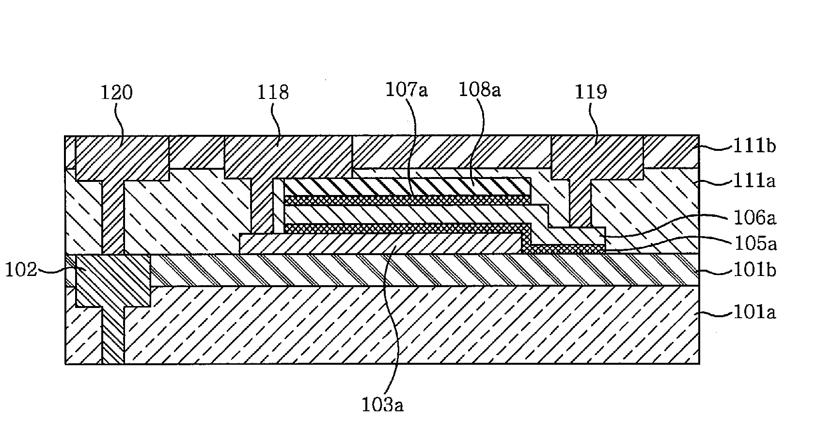
[0013]In general, example embodiments of the invention relate to a semiconductor device and a method for manufacturing the same, capable of obtaining a higher capacitance compared to area by connecting capacitors in parallel, facilitating a parallel connection of capacitors by using a metal trench, and reducing the area occupied by the semiconductor device.
[0014]In one example embodiment, a capacitor of a semiconductor device includes a first electrode, first dielectric layer, second electrode, second dielectric layer, and third electrode sequentially formed on a semiconductor substrate. The capacitor also includes a first contact coupled to the first electrode and to the third electrode. The capacitor further includes a second contact coupled to the second electrode.
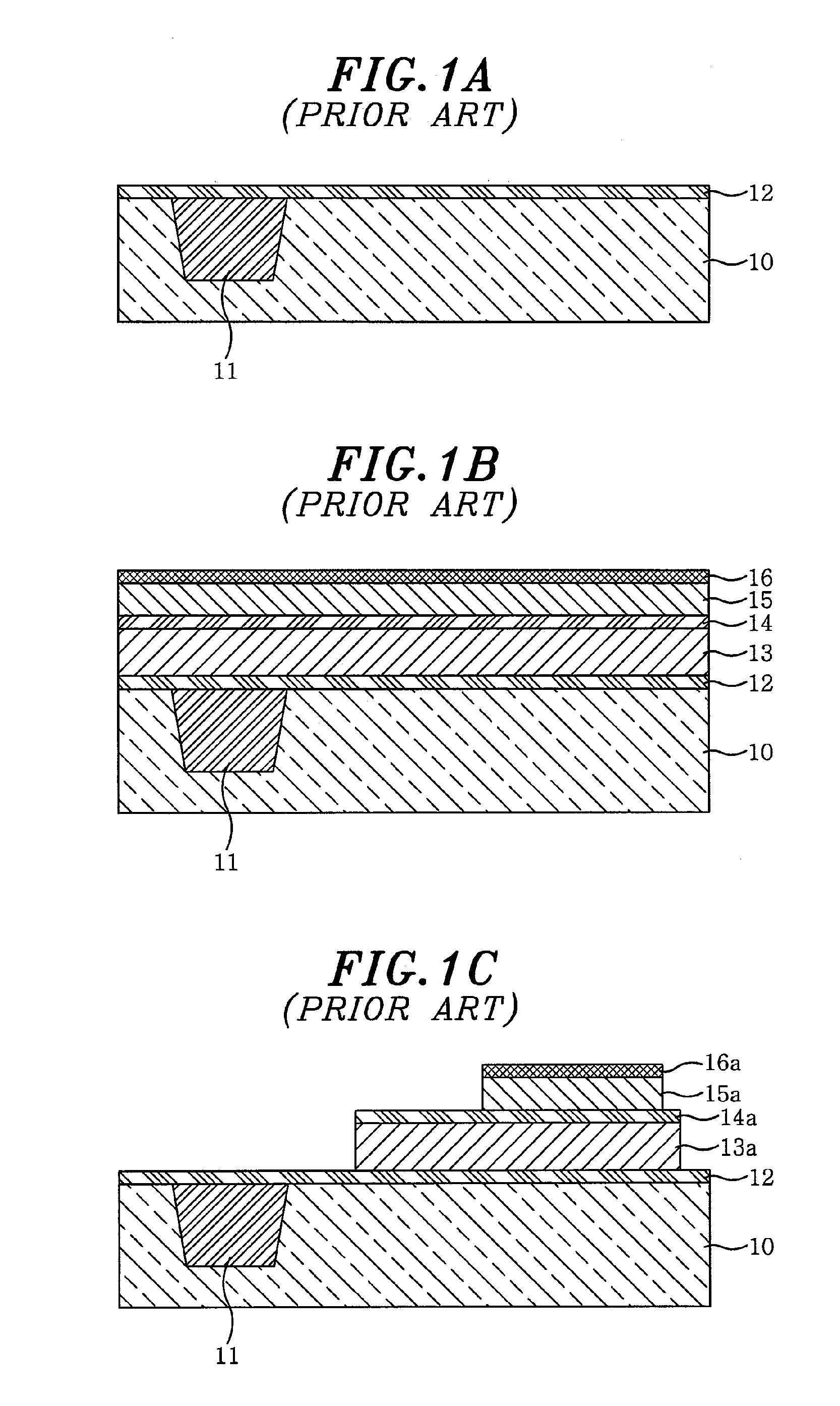
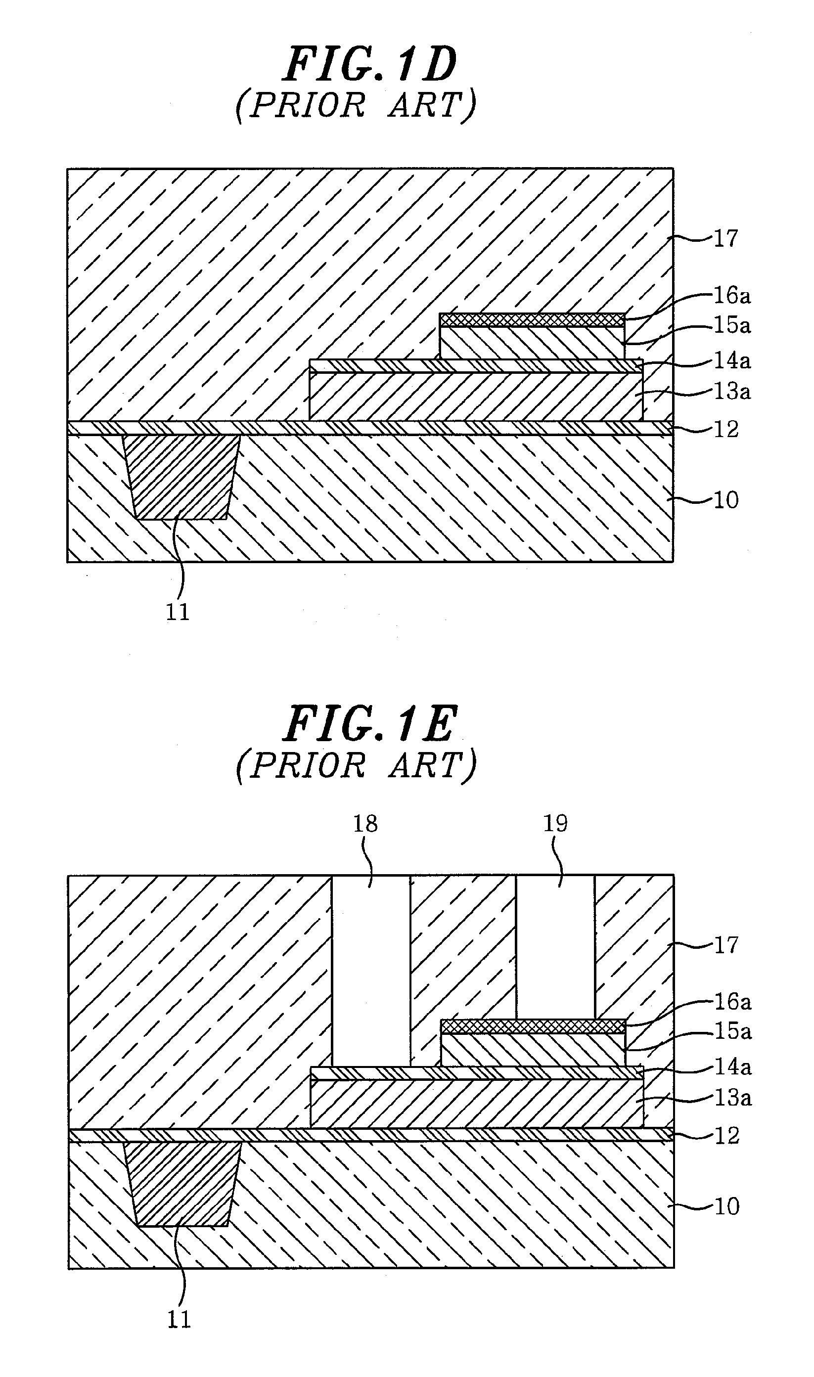
[0015]In another example embodiment, a method for manufacturing a semiconductor device includes various steps. First, a first electrode is formed by laminating a first conductive layer on a semiconductor substrate and e...
PUM
 Abstract
Description
Claims
Application Information