

Repair Structure and Method for Liquid Crystal Display
a liquid crystal display and repair structure technology, applied in non-linear optics, instruments, optics, etc., can solve the problems of inability to use conventional repair methods and repair structures, and easy failure of broken points
- Summary
- Abstract
- Description
- Claims
- Application Information
AI Technical Summary
Problems solved by technology
Method used
Image

Examples
first embodiment
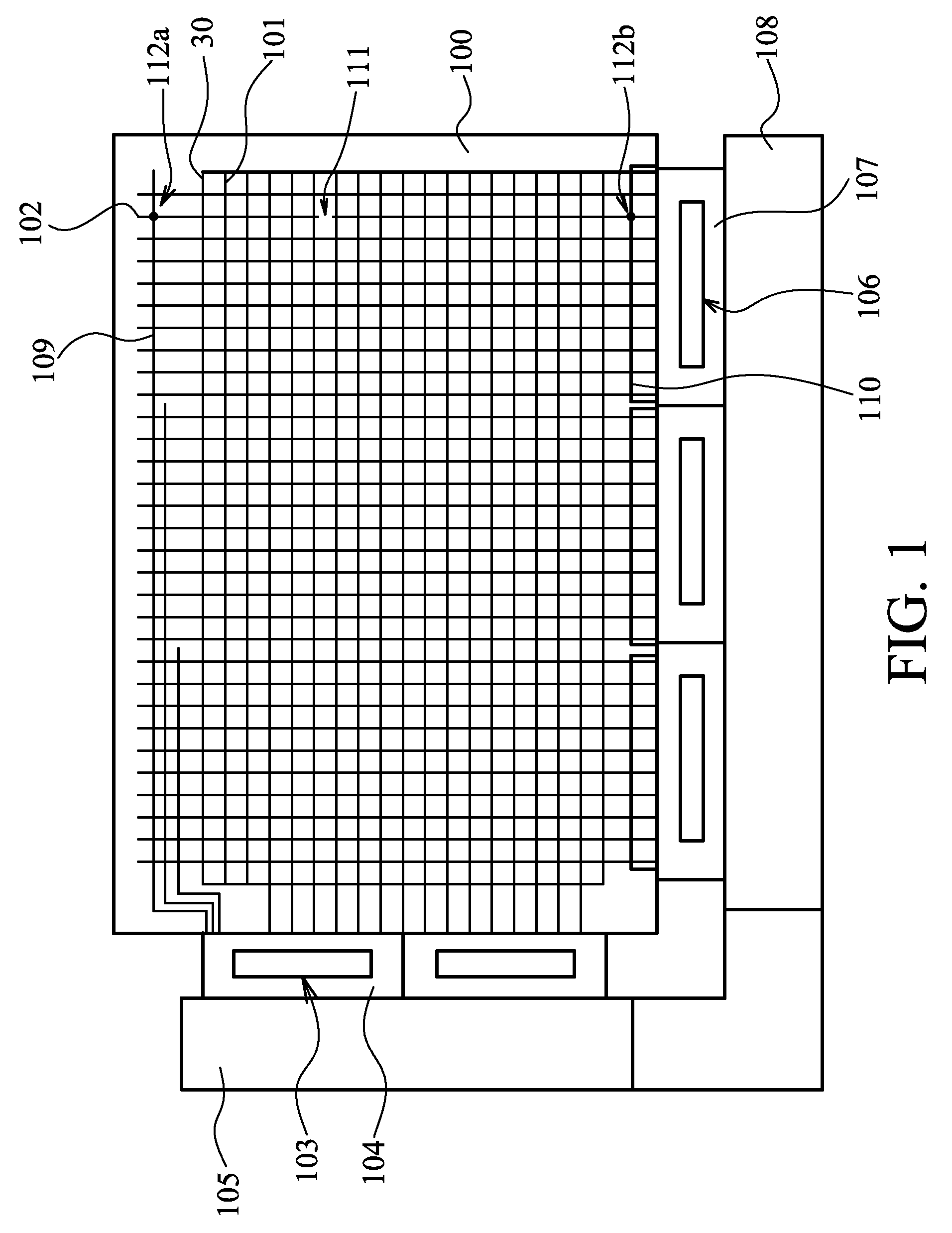
[0025]FIG. 2 shows a data line repair structure for a liquid crystal display panel according to the invention. Liquid crystal display panel 201, such as a glass baseboard, comprises scan line 202 and data line 203 crossing scan line 202. A thin film transistor (not shown in FIG. 2) is formed at an intersection of scan line 202 and data line 203. The thin film transistor comprises a gate coupled to scan line 202, a source coupled to data line 203 and a drain coupled to a pixel electrode (not shown). Gate driving chip 204 is connected by conductive glue to a Y side area of liquid crystal display panel 201, a chip-on-glass (COG) structure, and uses scan line 202 to transmit a gate signal to drive the thin film transistor. Source driving chip 205 is bound to flexible board 206a, a tape carrier package (TCP) structure, and uses data line 203 to transmit a data signal to write to the pixel electrode. One side of flexible board 206a is connected to liquid crystal display panel 201 and anot...
third embodiment
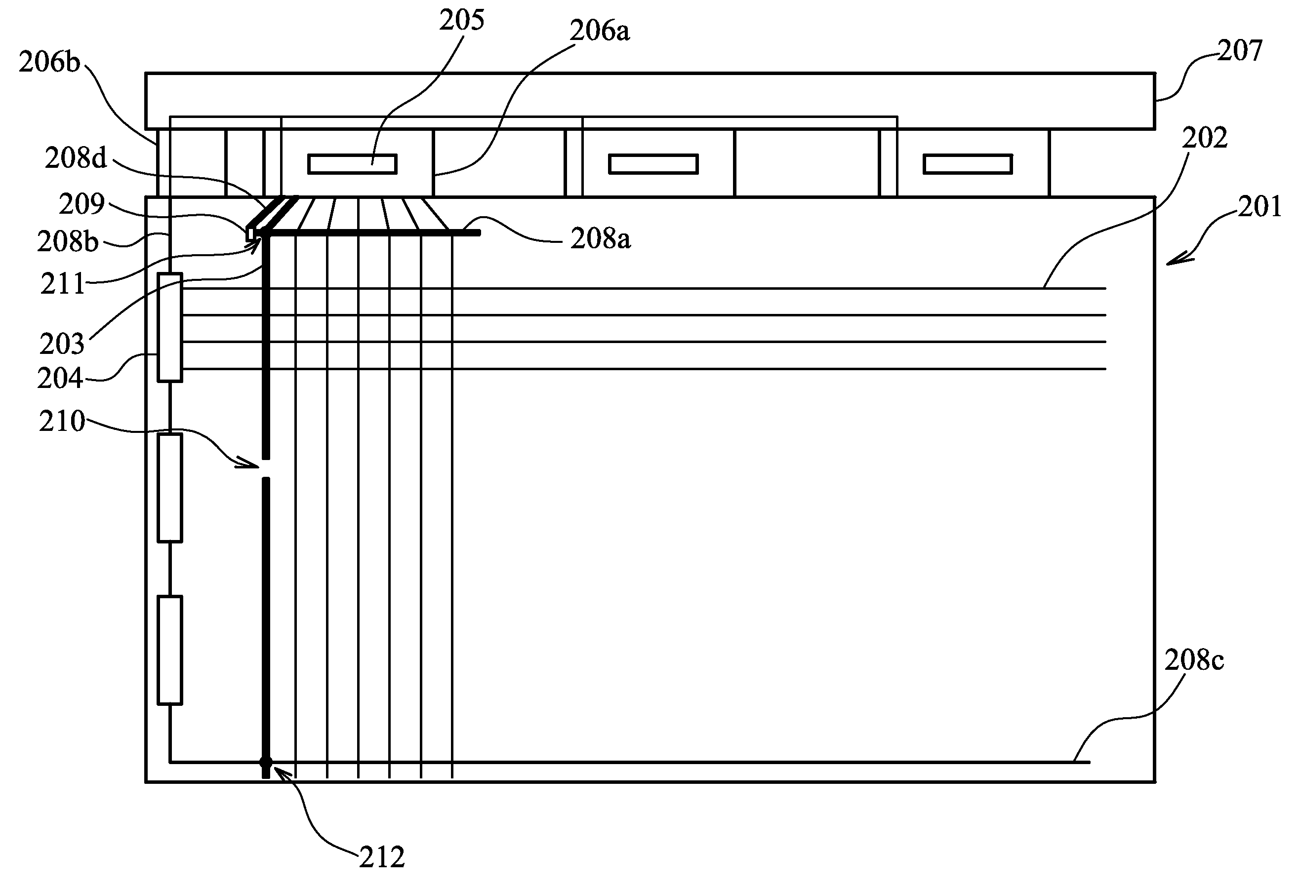
[0029]FIG. 3B shows a data line repair structure for a liquid crystal display panel according to the invention. A data signal generated by source driving chip 305 is transmitted through bypass circuit line 321 not inner circuits of gate driving chip 304. Thus, a data signal generated by source driving chip 305 is transmitted to data line below broken point 310 through first repair line 308a, fourth repair line 308d, flexible board 306c, lines of printed circuit board 307, flexible board 306b, second repair line 308b, flexible board 306a, bypass circuit line circuit line 321 and third repair line 308c, sequentially.
[0030]FIG. 4 shows a data line repair structure for a liquid crystal display panel according to a fourth embodiment of the invention. Liquid crystal display panel 401 is similar to the first embodiment of the invention, except that, here, source driving chip 405 uses conductive glue to connect with an X side area of liquid crystal display panel 401. Thus, the data line rep...
second embodiment
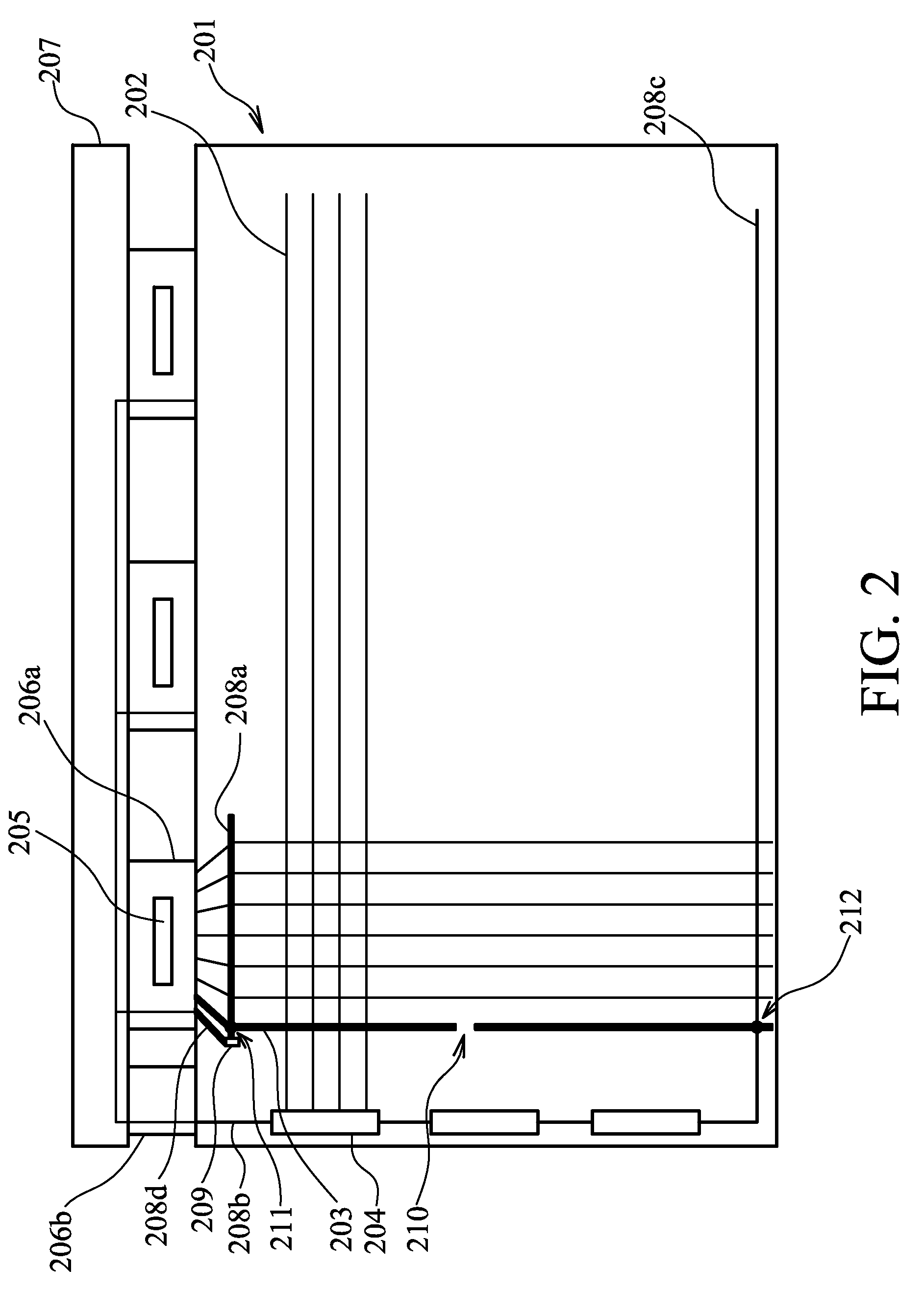
[0034]FIG. 7A shows a data line repair structure for a liquid crystal display panel according to another embodiment of the invention. Liquid crystal display panel 701 is similar to the invention shown in FIG. 3A, except that, here, floating lines 703 are added, and third repair line 308c is not crosses the end of data line 303 on the opposite side of source driving chip 305. Specifically, third repair line 308c is separated from the end of data line 303 on the opposite side of source driving chip 305. Floating line 703 crosses a portion of third repair line 308c and overlaps the end of data line 303, and is welded by a laser beam to connect the third repair line 308c with the end of data line 303 where data line 303 comprises broken point 310. A laser beam can be implemented to weld first repair line 308a and data line 303 to form connecting point 311, weld third repair line 308c and floating line 703 to form connecting point 705a, weld data line 303 and floating line 703 to form co...
PUM
 Abstract
Description
Claims
Application Information