Apparatus and Method for Treating Substrate

a technology of apparatus and substrate, applied in the direction of liquid surface applicators, pretreated surfaces, coatings, etc., can solve the problems of difficult to control the temperature of the wafers equally and precisely, the photoresist to be coated in a coating process with a low uniformity between wafers or between regions in a single wafer

Active Publication Date: 2009-05-28
SEMES CO LTD
View PDF7 Cites 4 Cited by
  • Summary
  • Abstract
  • Description
  • Claims
  • Application Information

AI Technical Summary

Benefits of technology

[0028]According to the present invention, it is possible to maintain the wafer at a process temperature while a process, such as a coating process or the like, is performed.
[0029]Also, according to the present invention, it is possible to eliminate a temperature difference from region to region within an entire region of a wafer while a process, such as a coating process or the like, is performed.
[0030]In addition, according to the present invention, it is not necessary to essentially provide a separate device for the temperature control of a wafer since the temperature control of the wafer is performed by a thinner supplied to the wafer before a photoresist is coated.

Problems solved by technology

Accordingly, it is not easy to control the temperature of the wafers equally and precisely.
The aforementioned drawback causes the photoresist to be coated in a coating process with a low uniformity between wafers or between regions in a single wafer.

Method used


Image

  • Apparatus and Method for Treating Substrate
  • Apparatus and Method for Treating Substrate
  • Apparatus and Method for Treating Substrate

Examples


Embodiment Construction

[0048]The present invention will now be described more fully with reference to the accompanying drawings, in which exemplary embodiments of the invention are shown. The invention may, however, be embodied in many different forms and should not be construed as being limited to the embodiments set forth herein; rather, these embodiments are provided so that this disclosure will be thorough and complete, and will fully convey the concept of the invention to those skilled in the art. In the drawings, the thicknesses of layers and regions are exaggerated for clarity.

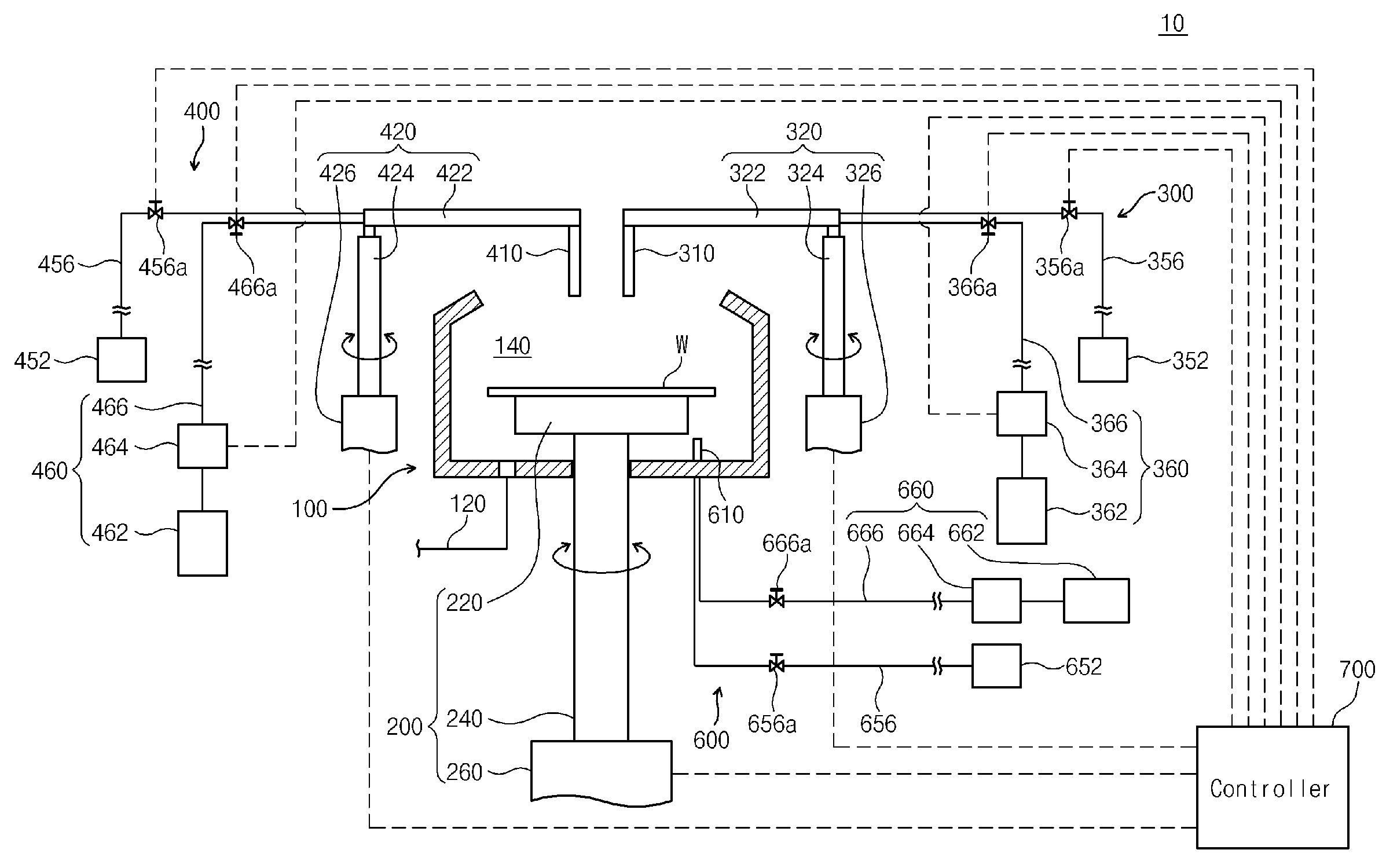
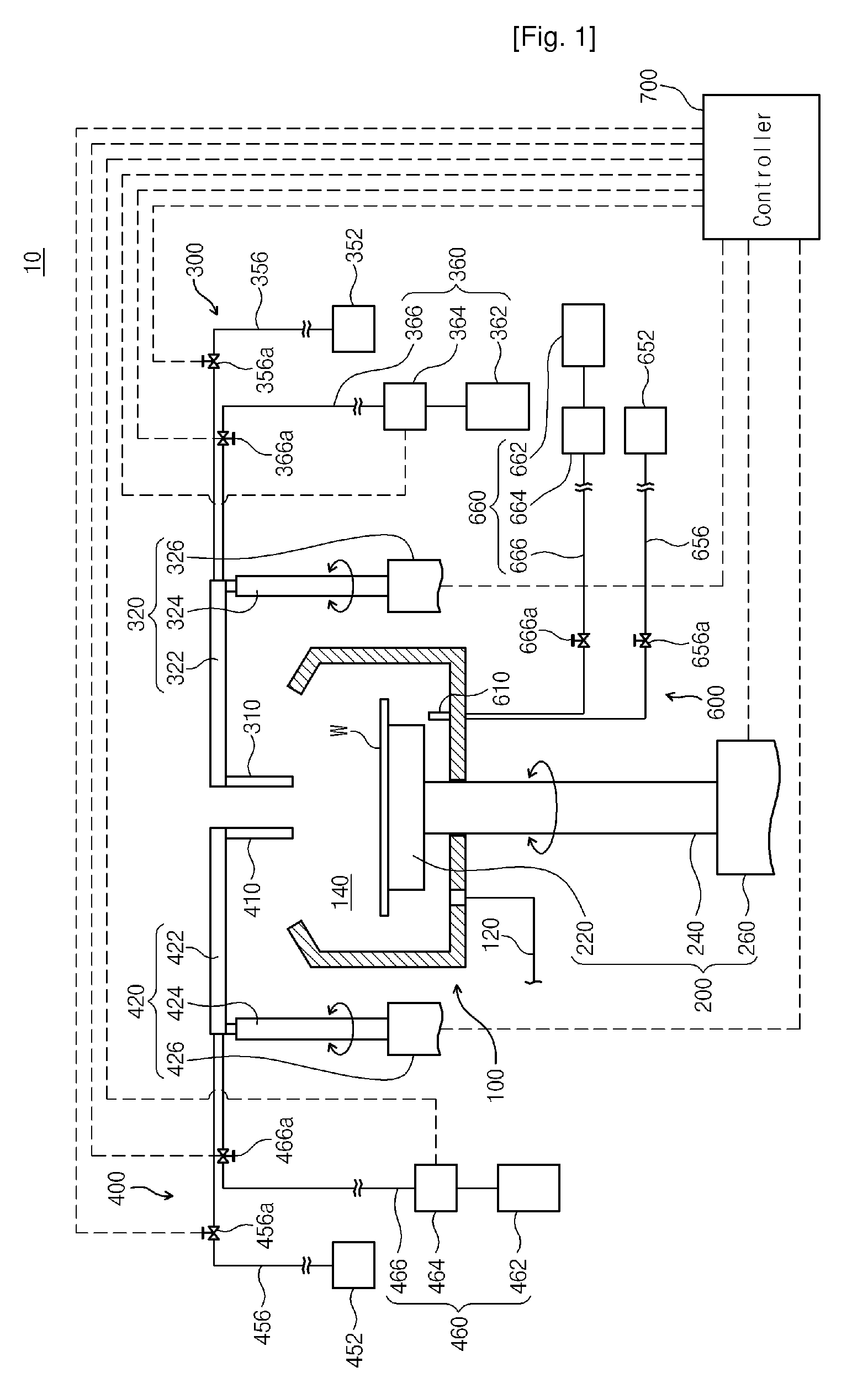
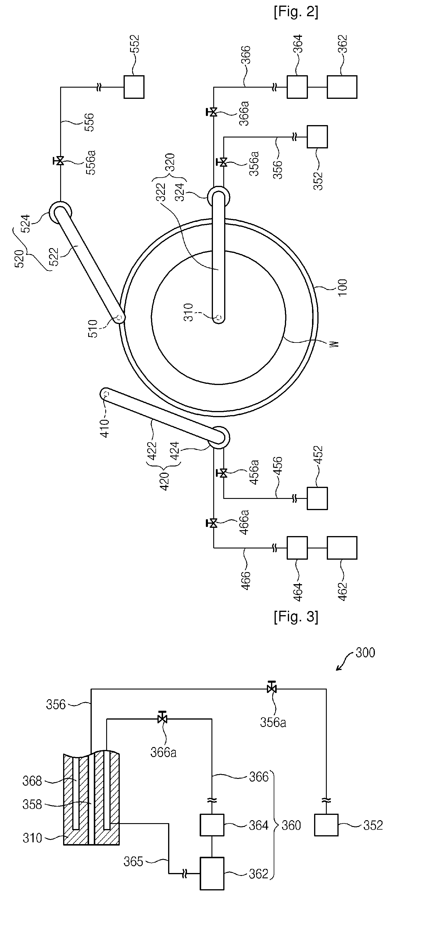
[0049]FIG. 1 is a view schematically showing an embodiment of a substrate treating apparatus 10 according to the present invention, and FIG. 2 is a plane view of FIG. 1. The present embodiment exemplarily illustrates an apparatus for coating a photoresist on a wafer W as one example of the substrate treating apparatus 10.

[0050]Referring to FIGS. 1 and 2, the coating apparatus according to the present invention has a container...


PUM


Abstract

The present invention provides a method that can maintain the temperature of a wafer at a process temperature before a coating process is performed by supplying a photoresist. According to the present invention, a thinner which helps a diffusion of the photoresist is supplied onto the wafer before the photoresist is supplied. The thinner is supplied in a temperature-controlled state such that the wafer has the process temperature by the thinner.

Description

TECHNICAL FIELD[0001]The present invention relates to apparatus and method for treating a substrate, and more particularly, to apparatus and method for treating a substrate, such as a semi-conductor substrate, by supplying a chemical onto the substrate.BACKGROUND ART[0002]For the fabrication of semiconductor devices, a wafer undergoes a variety of processes. Among these processes, a photolithography process is used to form a pattern on the wafer, and it includes a coating process of coating a photosensitive solution, such as a photoresist on the wafer, a photographing process of irradiating light onto the coated photoresist to form a provisional image for the pattern to be formed, and a developing process of developing the provisional image into the pattern. In the coating process, it is very important to coat the photoresist in a uniform thickness and at a set thickness, and the temperature of the wafer has a large influence on the thickness uniformity of the photoresist coated the...

Claims


Application Information

Patent Timeline
Patent Type & Authority Applications(United States)
IPC IPC(8): B05D3/10B05C5/00
CPCH01L21/67248H01L21/6708H01L21/304
Inventor CHOI, JONG-SUCHOI, YOUNG-KWEON
Owner SEMES CO LTD
Why Eureka
Try Eureka