Internal memory mapped external memory interface

Inactive Publication Date: 2009-05-28
APPLE INC
View PDF17 Cites 9 Cited by
  • Summary
  • Abstract
  • Description
  • Claims
  • Application Information

AI Technical Summary

Benefits of technology

[0006]This is directed to allowing a processor of a device to use ordinary internal memory read and write instructions to read and write to external memory. Thus, the complexities associated with the existing methods of accessing external memory can be avoided.

Problems solved by technology

However, the interface protocol is often comparatively complex.
This would in turn require that relatively complex software be executed at the processor in order to access external memory.

Method used


Image

  • Internal memory mapped external memory interface
  • Internal memory mapped external memory interface
  • Internal memory mapped external memory interface

Examples


Embodiment Construction

[0014]In the following description of preferred embodiments, reference is made to the accompanying drawings which form a part hereof, and in which it is shown by way of illustration specific embodiments in which the invention may be practiced. It is to be understood that other embodiments may be utilized and structural changes may be made without departing from the scope of the preferred embodiments of the present invention.

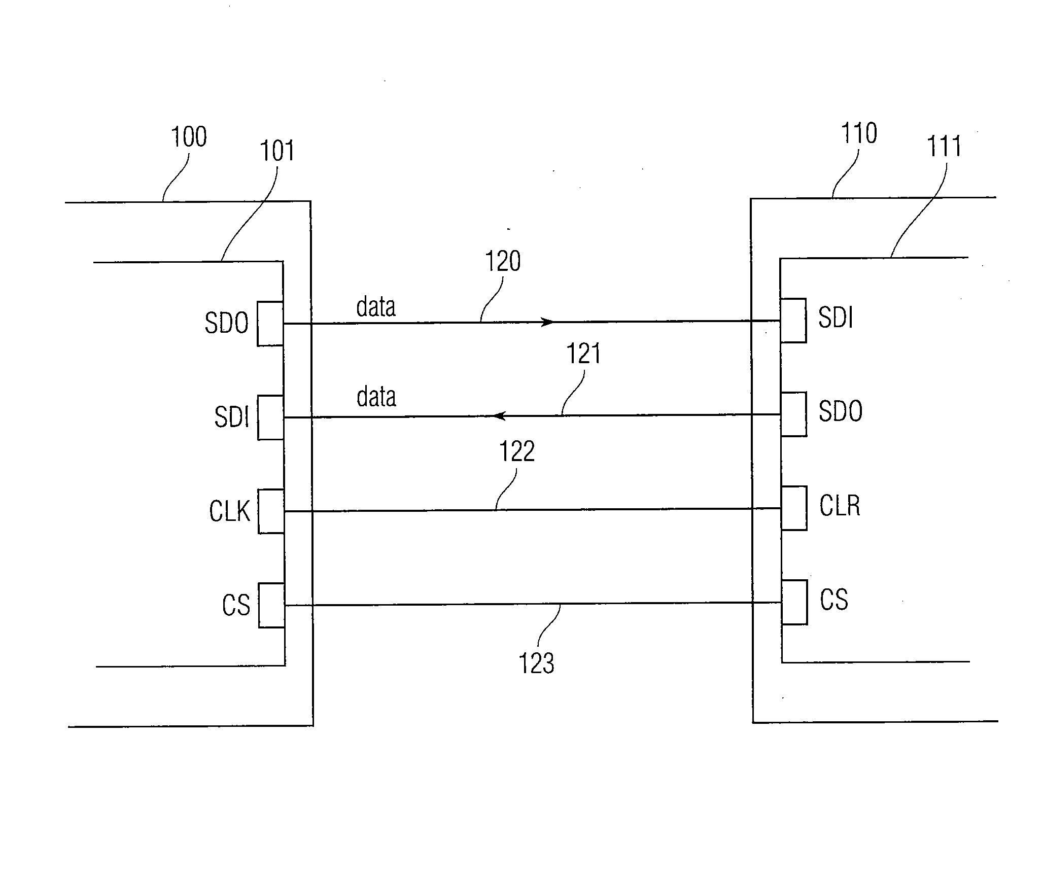
[0015]This relates to providing an external memory interface which allows for accessing external memory using internal memory access instructions and addressing.

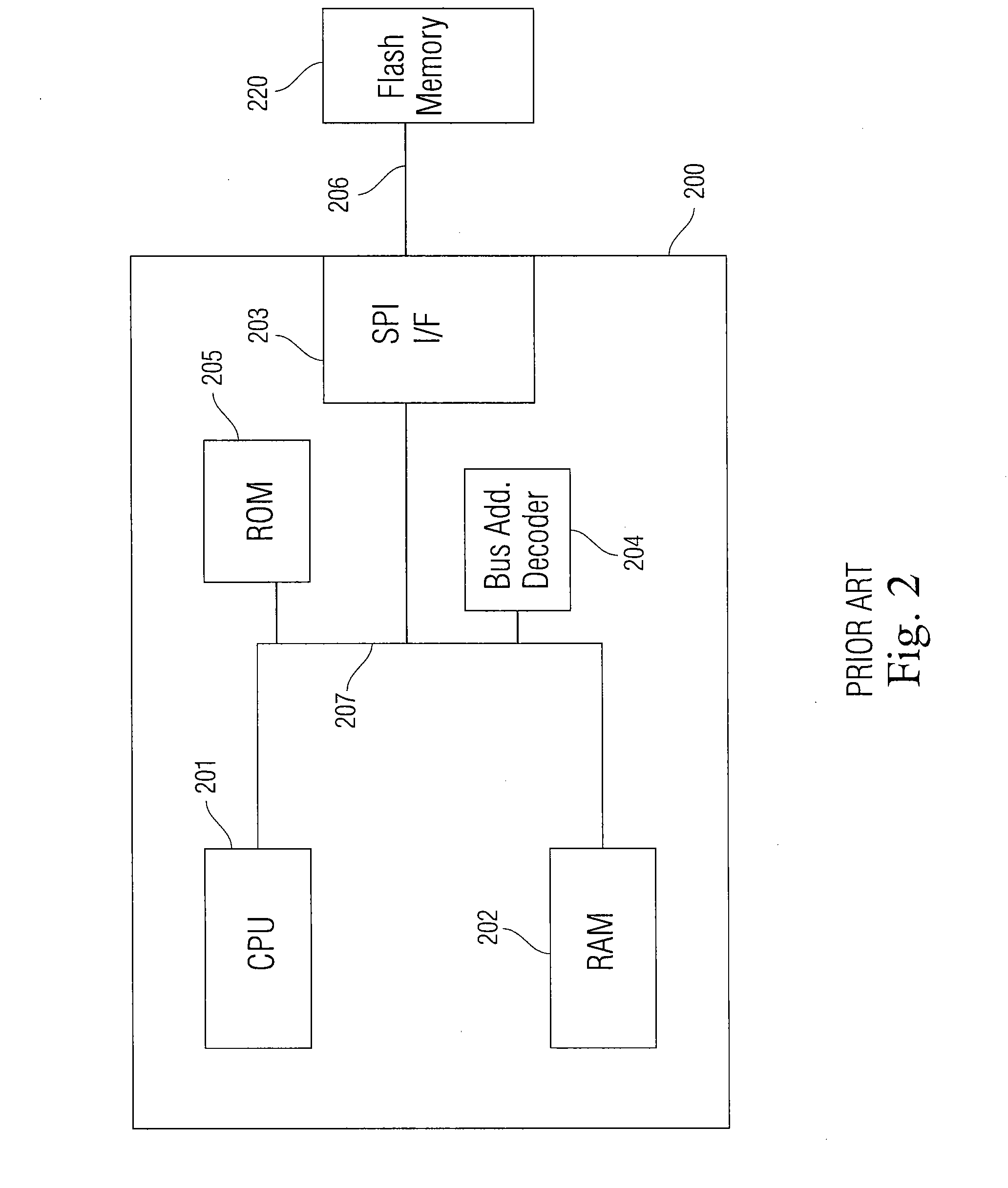
[0016]Although embodiments of the present invention are described herein in terms of FLASH memory accessed through the SPI interface, it should be understood that the present invention is not limited to these types of memory and this interface, but is generally applicable to all electronic devices that utilize an internal and external memory.

[0017]Embodiments of the present invention improve the efficienc...


PUM


Abstract

This is directed to allowing a processor of a device to use ordinary internal memory read and write instructions that read and write to external memory. Thus, the complexities associated with the existing methods of accessing external memory can be avoided. More specifically, an address space portion that does not correspond to any existing internal memory can be defined as associated with an external memory. When access to the external memory is required, the processor can simply issue ordinary internal memory read / write instructions that are addressed to the above mentioned address space. An interface controller can receive the read and write instructions and communicate with an external memory in order to execute them. The controller can then send a result back to the processor (if required) in the format that would be expected from an internal memory access operation.

Description

FIELD OF THE INVENTION[0001]This relates to devices utilizing external memories in general, and more specifically to using internal memory instructions for communication with external memories.BACKGROUND OF THE INVENTION[0002]Various existing electronic devices use a processor and a memory. The processor can execute instructions stored in the memory and process data stored in the memory. The processor usually accesses memory through an internal bus and references memory to be accessed using a single memory address space. Since memory access tends to occur very often, in many existing electronic devices the bus is designed to provide fast memory access based on simple instructions.[0003]Many electronic devices interact with external memories. Currently most popular external memories are FLASH based (such as, e.g., MEMORY STICK, COMPACT FLASH, SMART MEDIA, etc.) However other types of external memories can be used, such as volatile memory modules, hard drive modules, or floppy disk or...

Claims


Application Information

Patent Timeline
IPC IPC(8): G06F12/00
CPCG06F2212/2022G06F12/06
Inventor WILSON, THOMAS JAMESHORI, YUTAKA
Owner APPLE INC
Why Eureka
Try Eureka