Semiconductor device and method for manufacturing the same

a semiconductor and manufacturing method technology, applied in semiconductor devices, semiconductor/solid-state device details, electrical devices, etc., can solve the problems of complex flow of sealing resin, imperfect filling of sealing resin, fluidity deterioration, etc., and achieve the effect of stable quality

Active Publication Date: 2009-06-04
PANASONIC SEMICON SOLUTIONS CO LTD
View PDF6 Cites 50 Cited by
  • Summary
  • Abstract
  • Description
  • Claims
  • Application Information

AI Technical Summary

Benefits of technology

[0019]Therefore, with the foregoing in mind, it is an object of the present invention to provide a semiconductor device with stable quality, which can be manufactured without problems such as a shor

Problems solved by technology

Moreover, when the thermal conductor 119 as shown in FIG. 18 is included, the flow of the sealing resin is complicated and the fluidity det

Method used


Image

  • Semiconductor device and method for manufacturing the same
  • Semiconductor device and method for manufacturing the same
  • Semiconductor device and method for manufacturing the same

Examples


embodiment 1

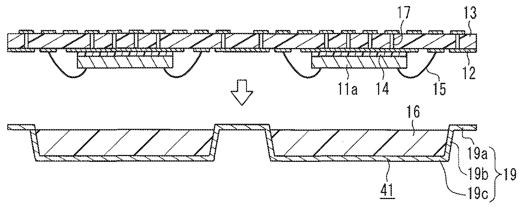
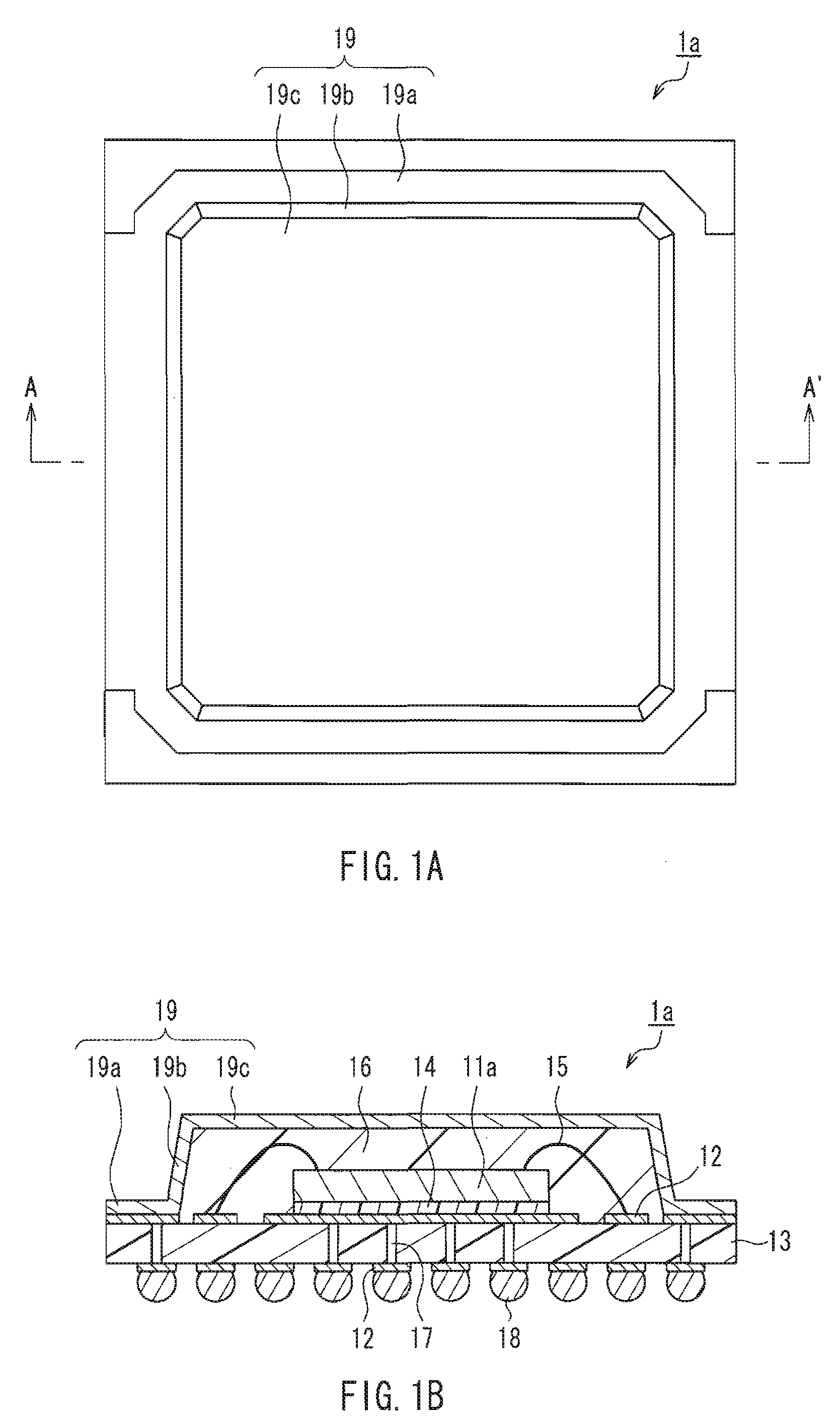
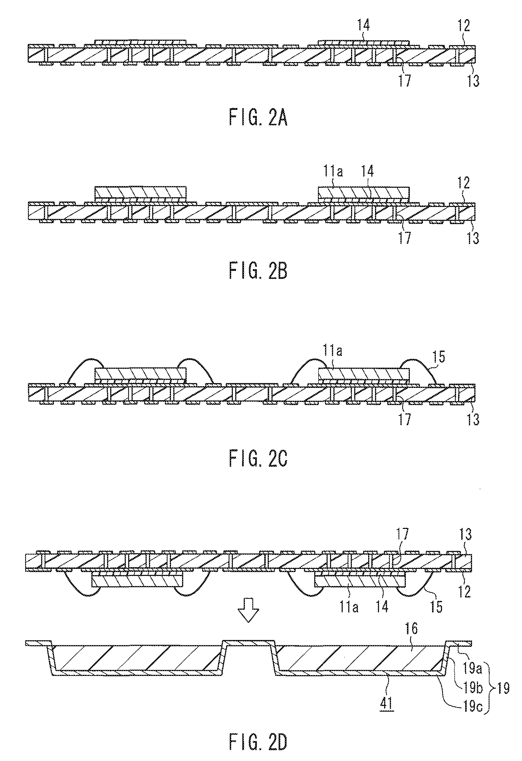
[0077]A configuration of a semiconductor device according to Embodiment 1 of the present invention will be described below. FIG. 1 includes views for showing the configuration of a semiconductor device 1a in Embodiment 1 of the present invention. FIG. 1A is a top view of the semiconductor device 1a, and FIG. 1B is a cross-sectional view taken along the line A-A in FIG. 1A.

[0078]As shown in FIG. 1B, wiring patterns 12 are formed on both surfaces of a substrate 13 made of an insulating resin. The wiring patterns 12 are connected electrically to each other through via holes 17. A semiconductor element 11a is adhered to the substrate 13 through an adhesive 14. An electrode is formed on the upper surface of the semiconductor element 11a and connected to the wiring pattern 12 through metal thin wires 15. A sealing resin 16 seals integrally the semiconductor-element-mounting surface of the substrate 13, the semiconductor element 11a, the adhesive 14 and the metal thin wires 15.

[0079]A ther...

embodiment 2

[0093]A semiconductor device according to Embodiment 2 of the present invention will be described below. FIG. 7A is a top view showing the configuration of a semiconductor device 2a in the present embodiment. FIG. 7B is a cross-sectional view taken along the line C-C′ in FIG. 7A. FIG. 7C is a cross-sectional view taken along the line D-D′ that is perpendicular to the line C-C′ in FIG. 7A. In the following description of embodiment, the same reference numerals may be assigned to the same components as those of the semiconductor device 1a in Embodiment 1 in order to avoid the duplication of explanations.

[0094]The thermal conductor 21 shown in FIG. 7B is made of a material having a preferable thermal conductivity, such as Cu, Cu alloy, Al, Al alloy and Fe—Ni alloy. The thermal conductor 21 includes a contact portion 21a, an inclined portion 21b formed with an inclination from the contact portion 21a, and a flat portion 21c formed continuously from the inclined portion 21b and in parall...

embodiment 3

[0103]A semiconductor device according to Embodiment 3 of the present invention will be described below. FIG. 10A is a top view showing a configuration of a semiconductor device 3 in Embodiment 3 of the present invention. FIG. 10B is a cross-sectional view taken along the line F-F′ in FIG. 10A. In the following description of embodiment, the same reference numerals may be assigned to the same components as those of the semiconductor device 1a in Embodiment 1 in order to avoid the duplication of explanations.

[0104]A semiconductor element 11c has an electrode formed on the lower surface (circuit-formation surface). Bumps 24 connect the electrode (not shown) on the semiconductor element 11c and a wiring pattern 12 on the semiconductor-element-mounting surface of the substrate 13. The spacing between the semiconductor element 11c and the substrate 13 is filled with a resin 25, except for the region where the bumps 24 are formed.

[0105]A thermal conductor 23 is made of a material having p...


PUM


Abstract

A method includes: mounting a plurality of semiconductor elements on a substrate having wirings; connecting electrically electrodes of the semiconductor elements and the wirings; sealing the semiconductor elements with a resin, which is carried out by bringing a thermal conductor having a concavity and the substrate to be in contact with each other so that the semiconductor elements are positioned within the concavity and by filling the concavity with the resin; and separating respective semiconductor elements 1. In the resin-sealing step, in a state where the thermal conductor is arranged with its concavity facing up and the concavity of the thermal conductor is filled with a liquid resin, the semiconductor elements are dipped in the liquid resin in the concavity and the liquid resin is solidified. Due to these steps, a semiconductor device can be manufactured without experiencing troubles such as short circuit of the metal thin wires or imperfect filling of resin during the manufacturing steps, and thus semiconductor devices with stable quality can be manufactured.

Description

BACKGROUND OF THE INVENTION[0001]1. Field of the Invention[0002]The present invention relates to a semiconductor device suitably used for a case in which semiconductor elements that generate much heat power are mounted, and a method for manufacturing the semiconductor device.[0003]2. Description of Related Art[0004]With the recent trend toward multifunction and reduction in size and thickness of electronic equipment, the semiconductor devices have become smaller and thinner, and the number of terminals tends to increase. For coping with this tendency, a so-called BGA (Ball Grid Array) package has been used. Unlike a conventional QFP (Quad Flat Package), a BGA package does not have an external lead protruding in the lateral direction. Instead, the BGA package has solder balls that are arranged in a matrix on the lower surface of a substrate and that serve as external electrodes for an electric connection with a mother board.[0005]Since it is expected that semiconductor elements gener...

Claims


Application Information

Patent Timeline
IPC IPC(8): H01L23/495H01L21/56H01L23/36
CPCH01L21/56H01L23/3128H01L23/3677H01L23/4334H01L24/97H01L2224/16H01L2224/32225H01L2224/48091H01L2224/48227H01L2224/73253H01L2224/73265H01L2224/97H01L2924/01013H01L2924/01029H01L2924/01057H01L2924/01082H01L2924/15311H01L2924/16152H01L24/48H01L2224/32245H01L2224/48247H01L2224/73204H01L2224/92125H01L2924/01005H01L2924/01006H01L2924/01033H01L2924/014H01L2224/16225H01L2924/07802H01L2224/85H01L2924/00014H01L2224/83H01L2224/92247H01L2924/00012H01L2224/81H01L2924/00H01L2224/451H01L24/45H01L24/73H01L2924/181H01L24/49H01L2224/49171H01L2224/05599
Inventor OHTANI, KATSUMI
Owner PANASONIC SEMICON SOLUTIONS CO LTD
Why Eureka
Try Eureka