Image processing device and image processing method

a technology of image processing and image processing, applied in the field of image processing device and image processing method, can solve the problems of not enabling the classification of shadows which appear when no light source is moved, and a large-scale device, and achieves the effect of easy extraction of attached shadow areas and casting shadow areas, high refinement of images, and high practicality

Active Publication Date: 2009-06-04
PANASONIC CORP
View PDF8 Cites 32 Cited by
  • Summary
  • Abstract
  • Description
  • Claims
  • Application Information

AI Technical Summary

Benefits of technology

[0017]According to the present invention, attached shadow areas and cast shadow areas are extracted using the polarization information of an object. In this way, it becomes possible to extract attached shadow areas and cast shadow areas from a snapshot-like image captured in a general environment without requiring a large-scale system enabling movement of a light source.
[0018]Therefore, the present invention makes it possibl

Problems solved by technology

However, Non-patent Reference 2 entails a problem of requiring an image of an object lighted by light sources in various directions and thus requires a large-scale device.
In addition, Non-patent Re

Method used


Image

  • Image processing device and image processing method
  • Image processing device and image processing method
  • Image processing device and image processing method

Examples


embodiment 1

[0079]First, a description is given of the outline of the optical area dividing device in Embodiment 1 of the present invention.

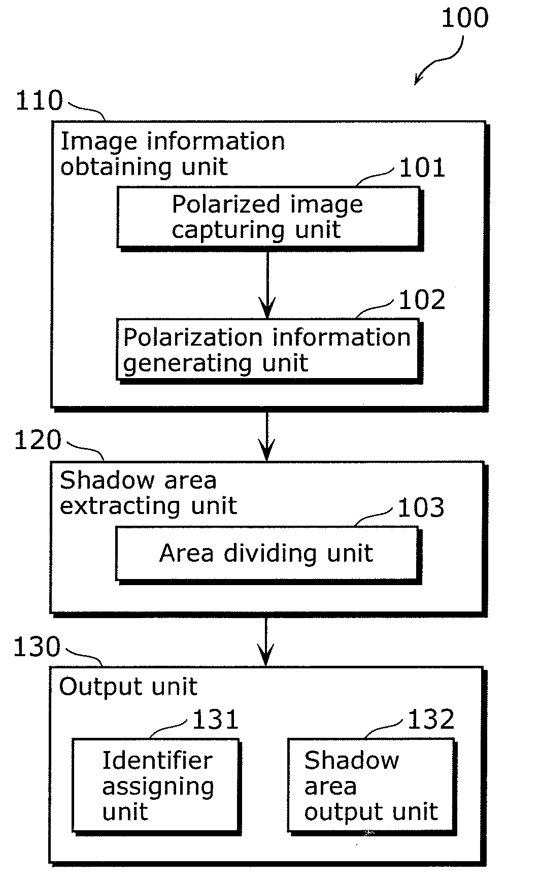
[0080]FIG. 1 is a functional block diagram showing the structure of the optical area dividing device 100 in this Embodiment. The optical area dividing device 100 is an example of the image processing device which performs processing on a shadow in the image of the object. Here, the optical area dividing device 100 is a device for performing optical area division on the surface of the object by imaging the object, and includes an image information obtaining unit 110, a shadow area extracting unit 120, and an output unit.

[0081]The image information obtaining unit 110 is a processing unit for obtaining information related to an object image including luminance information about luminance of light from the object, and polarization information about polarization of light from the object, and includes a polarized image capturing unit 101 and a polarization inform...

embodiment 2

[0189]Next, a description is given of an optical area dividing device in Embodiment 2 of the present invention.

FIG. 32 is a functional block diagram showing the structure of the optical area dividing device 100b in this Embodiment. This optical area dividing device 100b is a device for performing optical area division on the surface of an object by imaging the object, and is characterized by classifying low luminance areas into “attached shadow areas or low reflectance areas” and cast shadow areas. This optical area dividing device 100b includes an area dividing unit 1031 instead of the area dividing unit 103 in the optical area dividing device 100 shown in FIG. 1. Here, the normal vector information generating unit 1041 is also shown in this example of processing in which the result of processing by the optical area dividing device 100b is used. Although the normal vector information generating unit 1041 is not an essential structural element of the image processing device accordin...

embodiment 3

[0210]Next, a description is given of an optical area dividing device in Embodiment 3 of the present invention.

[0211]FIG. 37 is a functional block diagram showing the structure of the optical area dividing device 100c in this Embodiment. This optical area dividing device 100c is a device for performing optical area division on the surface of an object by imaging the object, and is characterized by generating normal vector information only when accurate normal vector information can be generated. This optical area dividing device 100c includes an imaging condition judging unit 106 in addition to the structure of the optical area dividing device 100 shown in FIG. 1. Here, a normal vector information generating unit 104 is also shown in this example of processing in which the result of processing performed by the optical area dividing device 100c is used. Although this normal vector information generating unit 104 is not an essential element of the image processing device according to ...


PUM


Abstract

The image processing device performs processing on a shadow in an image of an object, and includes: an image information obtaining unit obtaining information about an image of the object, the information including luminance information about luminance of light from the object and polarization information about polarization of the light from the object; a shadow area extracting unit extracting an attached shadow area and a cast shadow area from the image of the object based on the luminance information and the polarization information, the attached shadow area appearing on the surface of the object depending on an angle of incidence light, and the cast shadow area appearing on the surface of a material body other than the object when the light is blocked by the object; and an output unit outputting information identifying the attached shadow area and cast shadow area.

Description

CROSS REFERENCE TO RELATED APPLICATION[0001]This is a continuation application of PCT application No. PCT / JP2008 / 002163 filed Aug. 7, 2008, designating the United States of America.BACKGROUND OF THE INVENTION[0002](1) Field of the Invention[0003]The present invention relates to devices which perform processing on images of objects, and in particular to devices which perform processing on shadows.[0004](2) Description of the Related Art[0005]Recently, image processing methods using shadows have been widely performed. For example, Non-patent Reference 1 has proposed an approach for estimating the distribution of light from a light source of real lighting based on the luminance distribution in a cast shadow which is a “shadow” generated by a material body which is an object having a known shape. This approach is derived from the fact that the relationship between the light source, the object, and the shadow can be represented as a geometrical and optical model. When this concept is app...

Claims


Application Information

Patent Timeline
IPC IPC(8): G06T15/50G01B11/26G01J4/04G02B5/30G03B11/00G06T1/00G06V10/145H04N5/225H04N5/232H04N5/238
CPCG01B11/002H04N5/232G06T15/60G06K9/2036H04N5/2351G06V10/145H04N23/60H04N23/71
Inventor SATOKANAMORI, KATSUHIRONAKATA, MIKIYA
Owner PANASONIC CORP
Why Eureka
Try Eureka