Method of Forming Film, Film Forming Apparatus and Storage Medium

Inactive Publication Date: 2009-06-11
TOKYO ELECTRON LTD
View PDF7 Cites 2 Cited by
  • Summary
  • Abstract
  • Description
  • Claims
  • Application Information

AI Technical Summary

Benefits of technology

[0020]Accordingly, the present invention can be variously utilized. For example, when a seed layer is formed in a recess in order to form a wiring layer of a semiconductor device by a plating process, the method of the present inventi

Problems solved by technology

However, such demands have brought about new tasks.
Therefore, it is difficult to control a scattering direction of the atoms.
In other words, when an aspect ratio of the wiring groove (depth of wiring groove/opening width thereof) increases due to a decrease of the line width, it is difficult for the metal atoms to penetrate into the wiring groove or a via hole easily.
Thus, a step coverage therefor becomes poor and, also, there occur disconti

Method used


Image

  • Method of Forming Film, Film Forming Apparatus and Storage Medium
  • Method of Forming Film, Film Forming Apparatus and Storage Medium
  • Method of Forming Film, Film Forming Apparatus and Storage Medium

Examples


Example

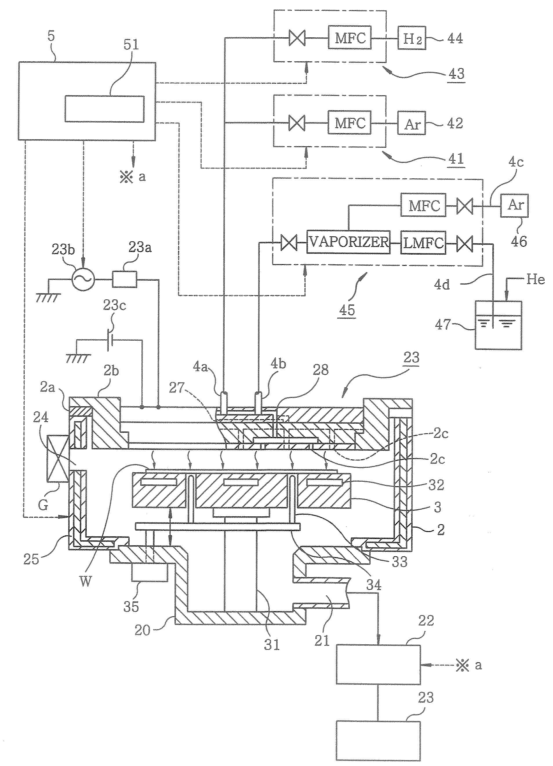
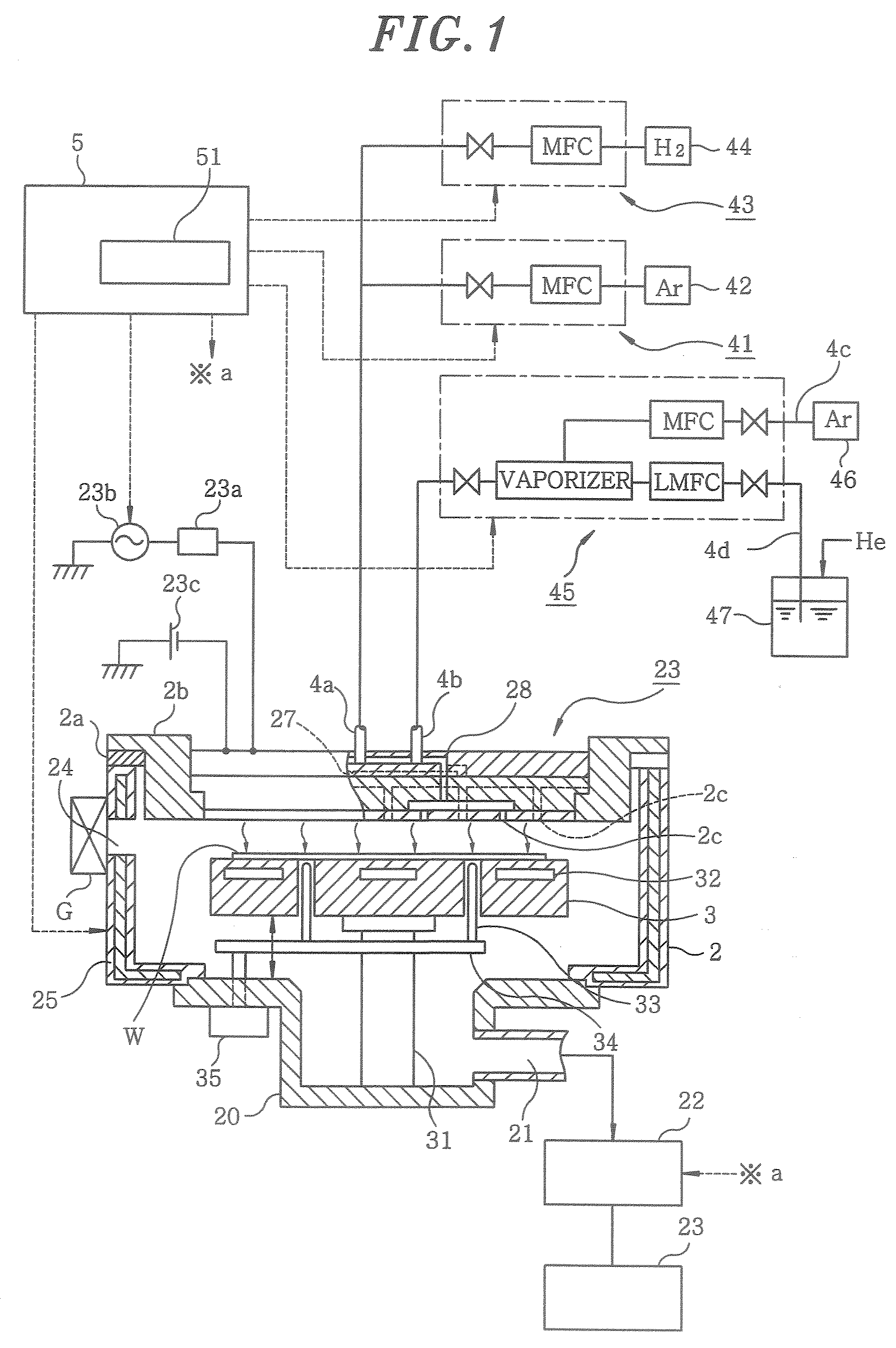
[0027]FIG. 1 shows an example of a film forming apparatus for performing a film forming method of the present invention. The film forming apparatus of the present invention forms a seed layer made of Cu (copper) on a surface of a wafer W, the wafer W being a target object. First, an entire configuration of the film forming apparatus will be described hereinafter.

[0028]As shown in FIG. 1, reference numeral 2 designates a processing chamber, where it has a recess 20 at the center of its bottom surface. A gas exhaust port 21 is formed on a sidewall of the recess 20 and communicates via a pressure control unit 22 with a vacuum pump 23 forming a vacuum exhaust unit together with the pressure control unit 22. Further, the pressure control unit 22 can maintain an inside of the processing chamber 2 at a specific vacuum pressure by, e.g., controlling an opening degree of a valve according to a control signal from a controller 5 to be described later. Moreover, an opening 24 that is openable / ...


PUM

PropertyMeasurementUnit
Thicknessaaaaaaaaaa
Forceaaaaaaaaaa
Frequencyaaaaaaaaaa

Abstract

Even in the application of a highly cohesive metal to a surface of treatment object having recesses of high aspect ratio, a continuous thin-film can be formed. There is provided a method of forming a film, comprising the step of carrying a substrate in a reaction chamber and mounting the same, the step of feeding a raw gas containing a compound of a first metal into the reaction chamber to thereby cause the surface of the substrate to adsorb the compound of the first metal, the step of bringing the compound the first metal into contact with a reducing plasma resulting from activation of a reducing gas to thereby obtain a first metal layer and the step of bringing a target electrode whose at least surface portion consists of a second metal different from the first metal into contact with a sputtering plasma and incorporating the thus ejected second metal into the first metal layer to thereby obtain an alloy layer, wherein this sequence of adsorption, reduction and alloy formation steps is carried out one or more times. By virtue of this method even when the cohesive force of the first metal is large, any migration thereof on the substrate is suppressed to thereby realize formation of a continuous thin film of small thickness.

Description

FIELD OF THE INVENTION[0001]The present invention relates to a film forming method and a film forming apparatus, each for forming a metal alloy thin film on a substrate, e.g., a semiconductor wafer or the like, and a storage medium for storing therein a program to execute the method.BACKGROUND OF THE INVENTION[0002]In a conventional semiconductor device such as an integrated circuit (IC) or the like, a wiring is formed on a semiconductor wafer (hereinafter, referred to as “wafer”) such as a silicon substrate or the like by burying a metal serving as a conductor in an insulating film such as a silicon oxide film (SiO2 film) or the like. As for a technique for forming the wiring, there is known one for burying a metal as a conductor in a wiring groove formed in an insulating film, e.g., a silicon oxide film or the like, formed on a surface of the silicon substrate and then removing an excess metal film by using a CMP (chemical mechanism polishing) method to thereby flatten a wafer sur...

Claims


Application Information

Patent Timeline
IPC IPC(8): C23C14/38
CPCC23C10/02C23C10/06C23C14/14C23C26/00H01L21/2855H01L21/28562H01L21/28556H01L21/76856H01L21/76873C23C14/0057H01J37/34C23C14/345C23C14/165H01L21/76843H01L21/203H01L21/205H01L21/285
Inventor YOSHII, NAOKIKOJIMA, YASUHIKO
Owner TOKYO ELECTRON LTD
Why Eureka
Try Eureka