Display substrate and method of manufacturing the same

Active Publication Date: 2009-06-11
SAMSUNG DISPLAY CO LTD
View PDF5 Cites 30 Cited by
  • Summary
  • Abstract
  • Description
  • Claims
  • Application Information

AI Technical Summary

Benefits of technology

[0012]According to the above description of one or more embodiments, when forming the organic semiconductor layer through an inkjet method, a bank pattern used for the organic semiconductor layer may be omitted. Acco

Problems solved by technology

When forming the organic semiconductor on the display substrate through the inkjet method, precise patterning of the organic semiconductor is difficult.
However, when forming the organic semiconductor on the display substrate by

Method used


Image

  • Display substrate and method of manufacturing the same
  • Display substrate and method of manufacturing the same
  • Display substrate and method of manufacturing the same

Examples


Example

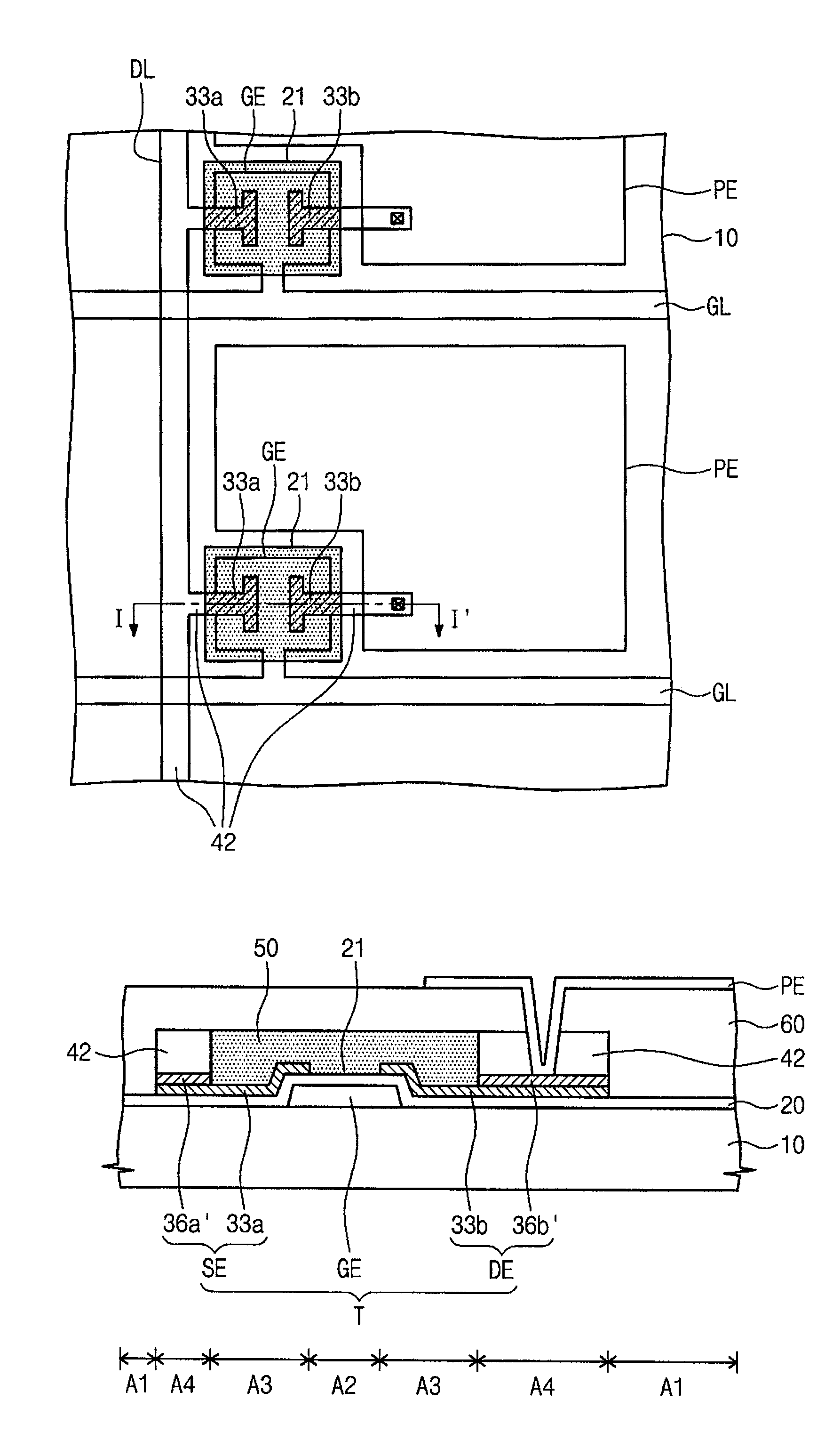
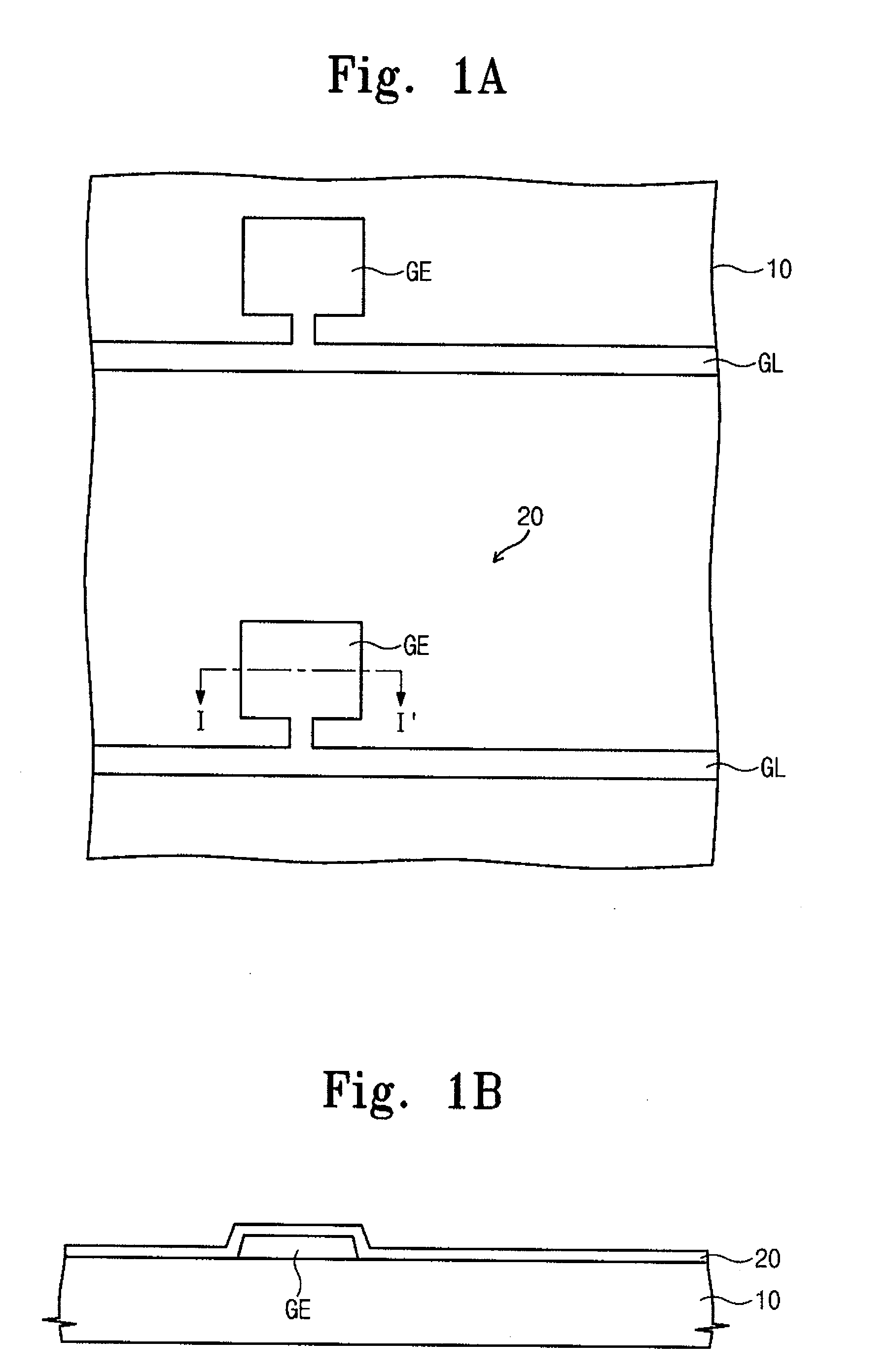
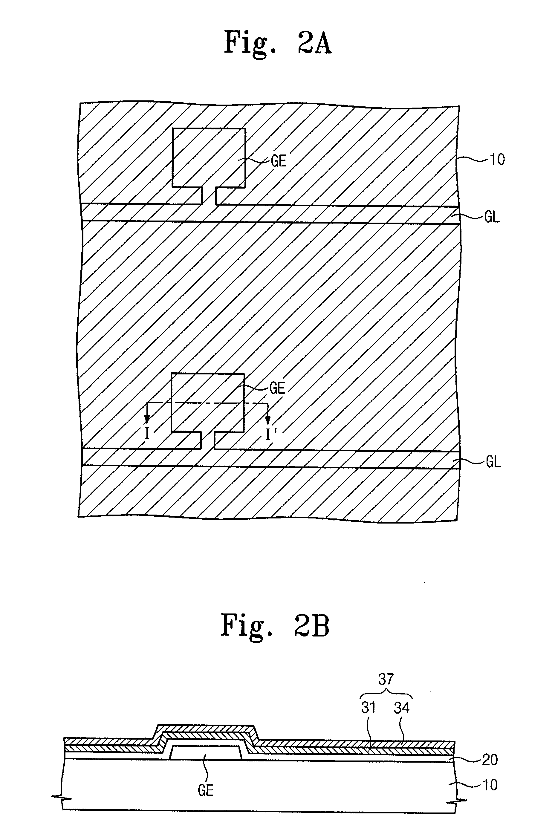
[0018]Hereinafter, embodiments of the present invention will be explained in detail with reference to the accompanying drawings. However, the scope of the present invention is not limited to such embodiments and the present invention may be realized in various forms. Embodiments of the present invention are defined only by the scope of the appended claims. In addition, the size of layers and regions shown in the drawings may be simplified or magnified for the purpose of clear explanation. In addition, the same reference numerals are used to designate the same elements throughout the drawings.

[0019]FIGS. 1A, 2A, 3A, 4A, 5A, 6A, 7A, 8A and 9A are plan views illustrating a method of manufacturing a display substrate according to one or more exemplary embodiments of the present invention, and FIGS. 1B, 2B, 3B, 4B, 5B, 6B, 7B, 8B and 9B are cross-sectional views taken along line I-I′ shown in FIGS. 1A, 2A, 3A, 4A, 5A, 6A, 7A, 8A and 9A, respectively, according to one or more embodiments....


PUM


Abstract

In a manufacturing method of a display substrate according to one or more embodiments, a plurality of thin films are patterned by using a photoresist film pattern having different thicknesses in each area on a substrate as etch masks. The photoresist film pattern may be etch-backed at least twice during the manufacturing process of the display substrate and may be used as the etch mask for patterns having shapes different from each other. Accordingly, the number of processes for manufacturing the mask patterns, which may be formed by a photolithography method in order to pattern the thin films formed on the substrate, may be reduced.

Description

CROSS-REFERENCE TO RELATED APPLICATION[0001]This application claims priority to and benefit from Korean Patent Application No. 2007-0126784 filed on Dec. 7, 2007, the contents of which are herein incorporated by reference in their entirety.BACKGROUND[0002]1. Technical Field[0003]Embodiments of the present invention generally relate to a display substrate and a method of manufacturing the display substrate.[0004]2. Description of the Related Art[0005]In general, a display apparatus that displays an image includes a display substrate. A plurality of pixel areas that displays an image is defined in the display substrate. Each pixel area includes a thin film transistor and a pixel electrode electrically connected to the thin film transistor.[0006]The thin film transistor includes a semiconductor pattern to selectively provide the pixel electrode with a pixel voltage according to a voltage applied to a gate electrode thereof. The semiconductor pattern includes an organic semiconductor su...

Claims


Application Information

Patent Timeline
IPC IPC(8): H01L51/05H01L51/40
CPCH01L27/283H01L51/0512H01L51/0023H01L51/0005H10K19/10H10K71/135H10K71/621H10K10/462G02F1/136
Inventor KIM, YOUNG-MINCHOI, TAE-YOUNG
Owner SAMSUNG DISPLAY CO LTD
Why Eureka
Try Eureka