Spin Transistor Using Epitaxial Ferromagnet-Semiconductor Junction

a technology of ferromagnet and junction, applied in the field of spin transistor, can solve the problems of difficult implementation of this earlier spin transistor in a large-scale device, physical limit of gate oxide film, and reduce the power consumption and area of electronic devices, and achieve the effect of low interface heterogeneity, miniaturization and large-scale integration

Inactive Publication Date: 2009-06-18
KOREA INST OF SCI & TECH
View PDF3 Cites 15 Cited by
  • Summary
  • Abstract
  • Description
  • Claims
  • Application Information

AI Technical Summary

Benefits of technology

[0008]The present invention is designed to solve the problems of the prior art, and therefore it is an object of the present invention to provide a spin transistor that is conducive to miniaturization and large scale integration and has low interface heterogeneity between a semiconductor substrate and ferromagnetic source and drain.

Problems solved by technology

In MOSFET, it is difficult to reduce the power consumption and area of the electronic device, and there is a physical limit on the gate oxide film.
Implementation of this earlier spin transistor in a large scale device has been difficult, and this spin transistor has problems (for example, low spin injection efficiency) caused by the heterogeneity in the interface of the semiconductor (a substrate) and the ferromagnets (a source and a drain).

Method used


Image

  • Spin Transistor Using Epitaxial Ferromagnet-Semiconductor Junction
  • Spin Transistor Using Epitaxial Ferromagnet-Semiconductor Junction
  • Spin Transistor Using Epitaxial Ferromagnet-Semiconductor Junction

Examples


Embodiment Construction

[0030]Exemplary embodiments of the present invention will now be described in detail with reference to the accompanying drawings. However, it should be understood that the detailed description and specific examples, while indicating preferred embodiments of the invention, are given by way of illustration only, since various changes and modifications within the spirit and scope of the invention will become apparent to those skilled in the art from this detailed description.

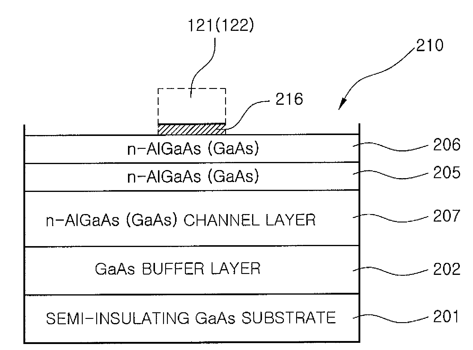
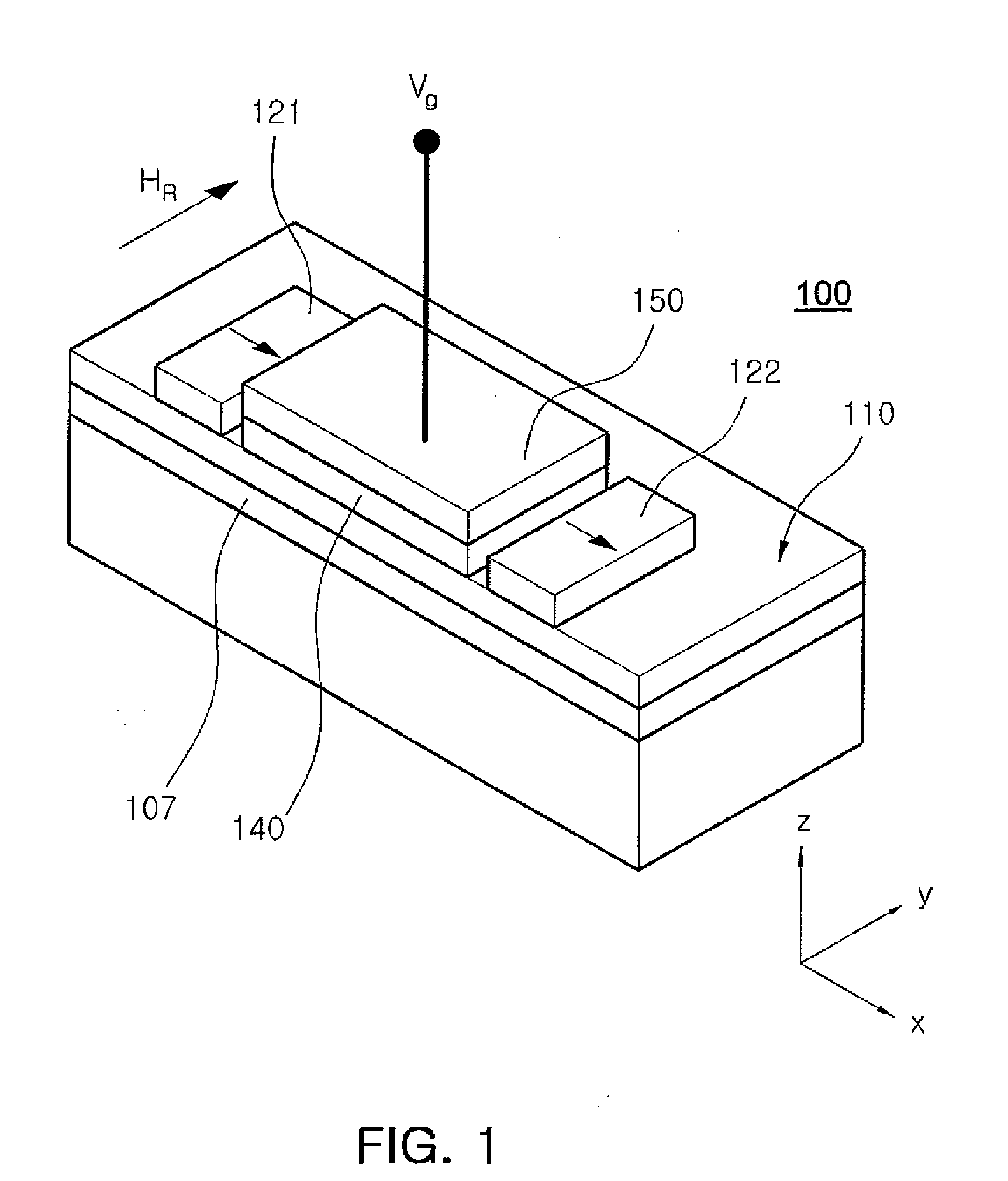
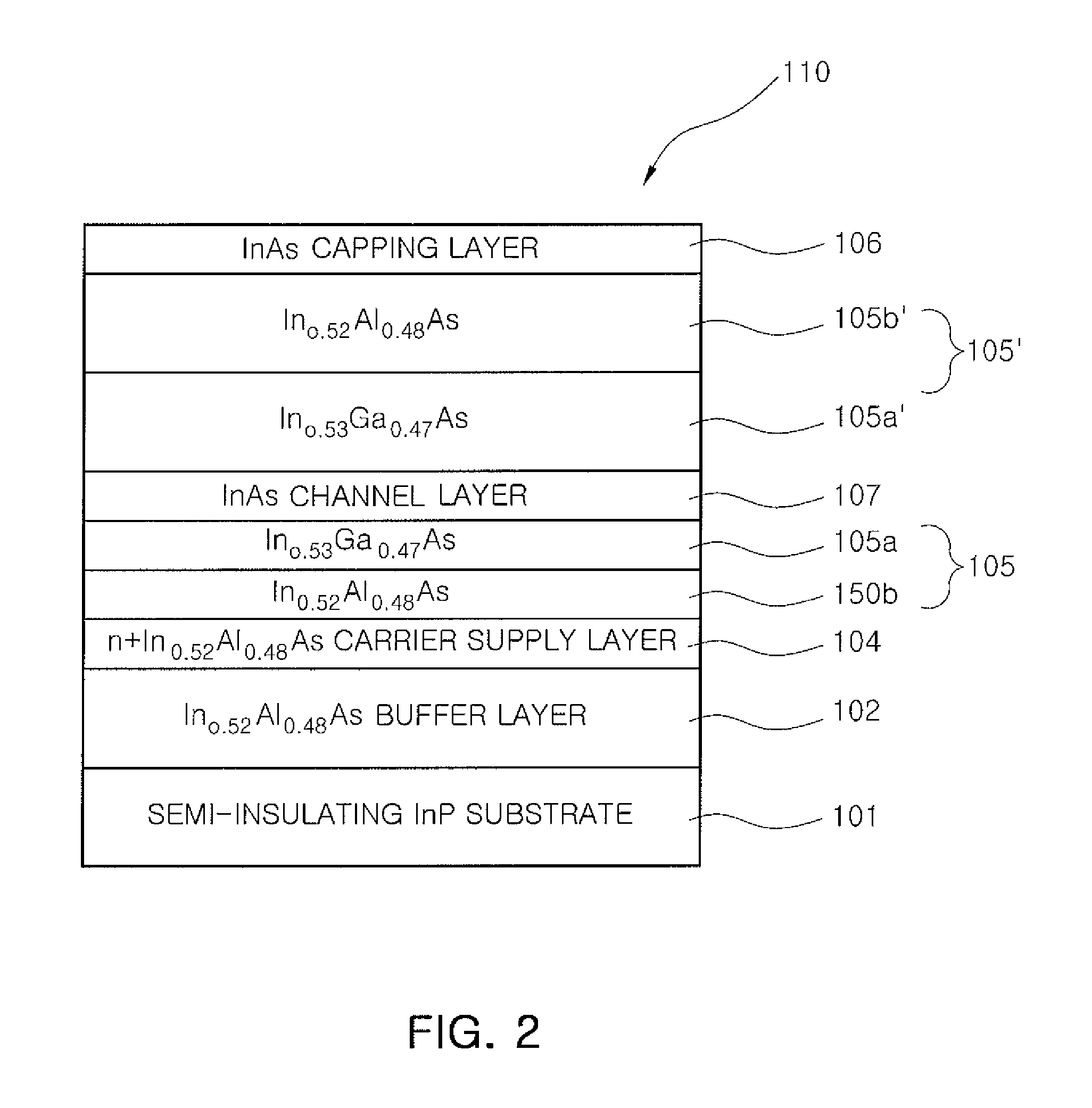
[0031]FIG. 1 is a perspective view illustrating a spin transistor according to one exemplary embodiment of the present invention. Referring to FIG. 1, the spin transistor 100 includes a semiconductor substrate 110 including a channel layer 107; and ferromagnetic source 121 and drain 122 disposed on the semiconductor substrate 110 to be spaced apart from each other. A gate 150 is formed between the source 121 and the drain 122 and disposed on the semiconductor substrate 110. The gate 150 is insulated from the semico...


PUM


Abstract

A spin transistor conducive to the miniaturization and large scale integration of devices, because a magnetization direction of a source and a drain is determined by a direction of the epitaxial growth of a ferromagnet. The spin transistor includes a semiconductor substrate having a channel layer formed thereinside; ferromagnetic source and drain epitaxially grown on the semiconductor substrate and magnetized in a longitudinal direction of the channel layer due to magnetocrystalline anisotropy—the source and drain being disposed spaced apart from each other in a channel direction and magnetized in the same direction—; and a gate disposed between the source and the drain to be insulated with the semiconductor substrate and formed on the semiconductor substrate to control the spin of electrons that are passed through the channel layer.

Description

CROSS-REFERENCE TO RELATED APPLICATIONS[0001]This application claims the priority of Korean Patent Application No. 2007-129952 filed on Dec. 13, 2007, in the Korean Intellectual Property Office, the disclosure of which is incorporated herein by reference.BACKGROUND OF THE INVENTION[0002]1. Field of the Invention[0003]The present invention relates to a spin transistor, and more particularly, to a spin transistor that is conducive to the miniaturization and large scale integration of devices, because a magnetization direction of a source and a drain is determined by a direction of the epitaxial growth of a ferromagnet.[0004]2. Description of the Related Art[0005]Most integrated circuit technologies include devices manufactured utilizing metal oxide semiconductor field effect transistor (MOSFET) technology. In addition, memory devices such as a dynamic random access memory (DRAM), or flash memory, application-specific integrated circuits (ASIC) microprocessors, and logic circuits also ...

Claims


Application Information

Patent Timeline
Patent Type & Authority Applications(United States)
IPC IPC(8): H01L29/51H01L21/00
CPCB82Y10/00H01L29/66984H01L29/205H01L29/122Y10S977/933H01L27/105H01L29/82
Inventor KOO, HYUN CHEOLHAN, SUK HEECHANG, JOON YEONKIM, HYUNG JUNKIM, KYUNG HO
Owner KOREA INST OF SCI & TECH
Why Eureka
Try Eureka