Nonvolatile semiconductor memory with erase gate and its manufacturing method

a technology of erase gate and semiconductor memory, which is applied in the direction of semiconductor devices, electrical appliances, basic electric elements, etc., can solve the problems of impeded high-speed erase operation and inability to improve erasure speed, so as to reduce capacitance coupling, improve erasure efficiency, and eliminate excess capacitance coupling between erase gate and floating gate

Inactive Publication Date: 2009-07-02
RENESAS ELECTRONICS CORP
View PDF8 Cites 27 Cited by
  • Summary
  • Abstract
  • Description
  • Claims
  • Application Information

AI Technical Summary

Benefits of technology

[0014]The erase gate in the present invention is formed opposite the edge of the lower surface of the floating gate and is positioned lower than the upper surface of the floating gate. Excessive capacitive coupling between the erase gate and floating gate can therefore be eliminated. Lowering the capacitive coupling between the erase gate and floating gate improves the erasure efficiency and speeds up the erasure operation. In other words, both the read speed and the erase speed are improved.

Problems solved by technology

However, coupling capacitance between this type of erase gate and floating gate acts to impede high-speed erase operation.
In other words, the erasure speed cannot be improved while on the other hand preventing a drop in the read speed.

Method used


Image

  • Nonvolatile semiconductor memory with erase gate and its manufacturing method
  • Nonvolatile semiconductor memory with erase gate and its manufacturing method
  • Nonvolatile semiconductor memory with erase gate and its manufacturing method

Examples


first exemplary embodiment

[0051]1. Structure

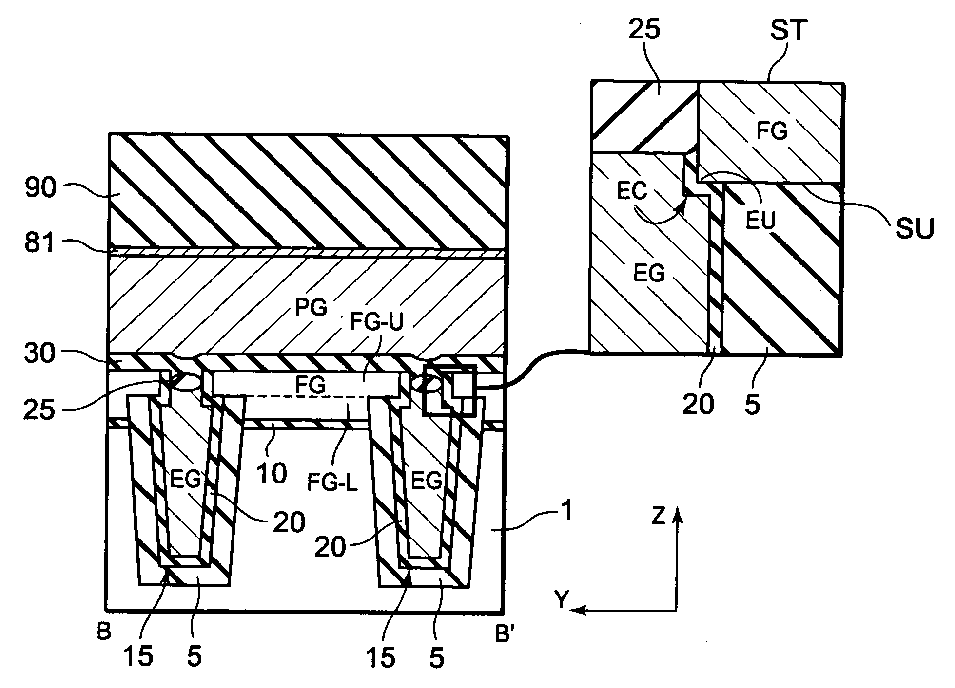
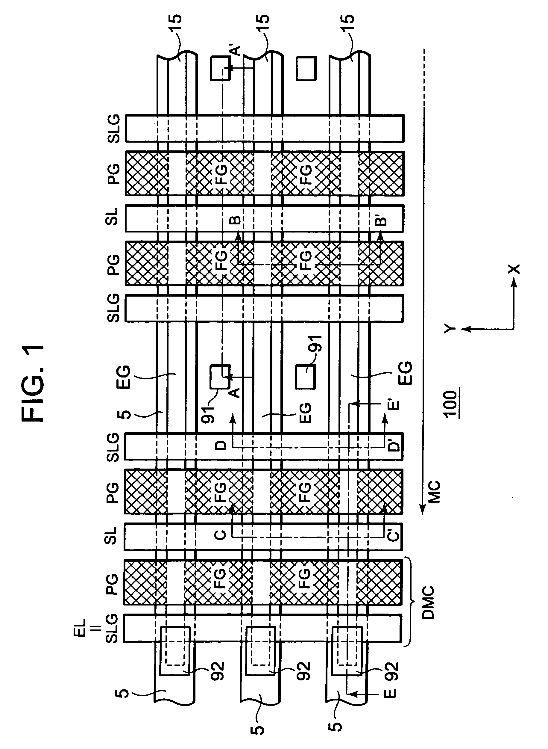
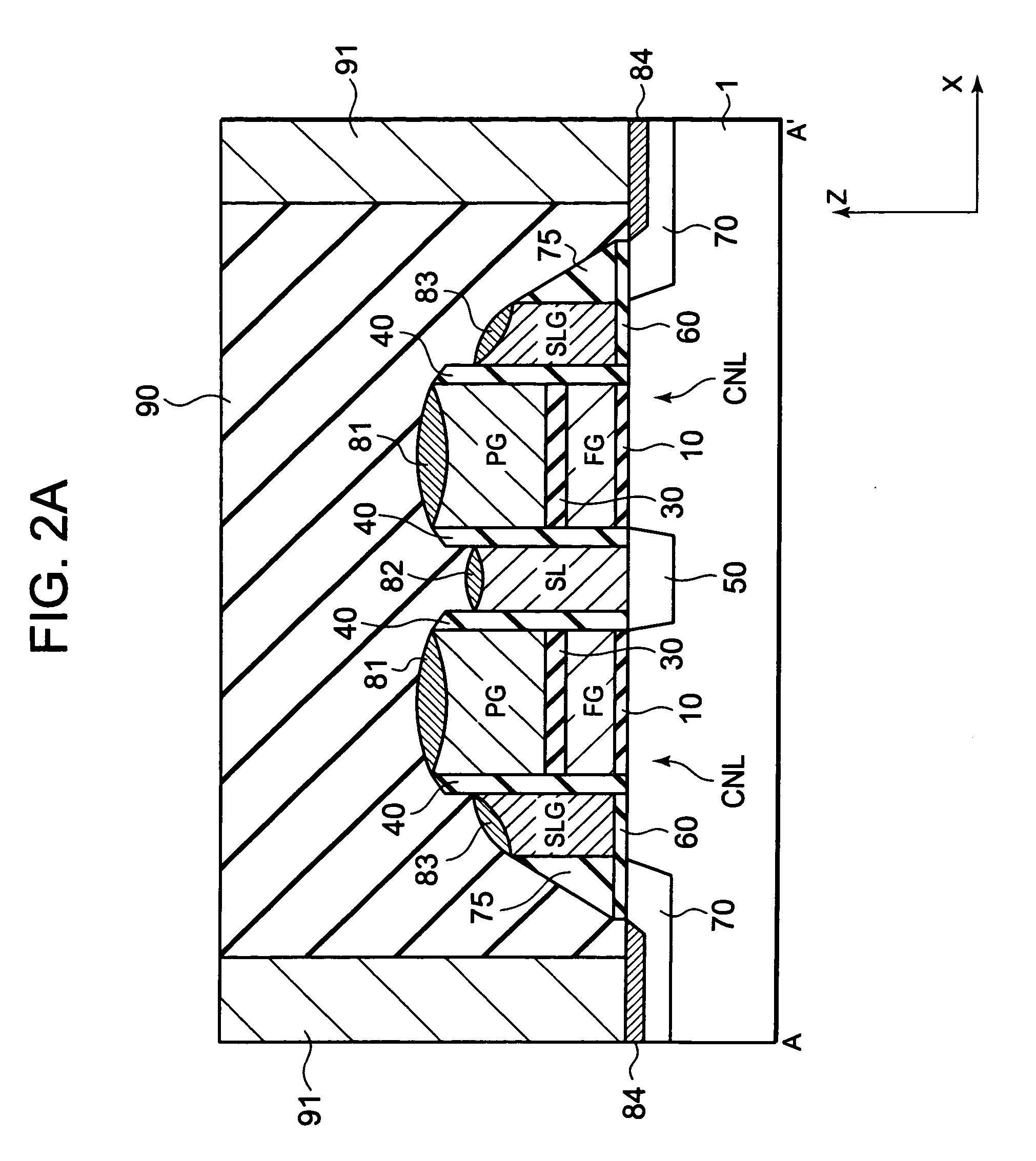
[0052]FIG. 1 is a plan view showing an overall structure of a nonvolatile semiconductor memory device of the first exemplary embodiment of this invention. FIG. 1 shows an approximate placement and extension direction of each gate, and an upper wiring layer is omitted from the drawing. The nonvolatile semiconductor memory device of the first exemplary embodiment includes a memory cell array 100 made up of multiple memory cells MC formed in arrays. Each of the memory cells MC is a field-effect transistor (FET) (memory cell transistor) containing multiple gates. More specifically, each memory cell MC contains an erase gate EG, a select gate SLG, a program gate PG, a floating gate FG, and a source line SL.

[0053]The erase gate EG is a gate for data erasure. The erase gate EG extends along the X direction as shown in FIG. 1. More specifically, the erase gate EG is formed along a device isolation structure formed to extend in the X direction. This device isolation structu...

second exemplary embodiment

[0117]In the second exemplary embodiment of this invention, there is no program gate PG. The same reference numerals are assigned to the same structures as in the first exemplary embodiment, and redundant descriptions are omitted.

[0118]FIG. 24 is a plan view showing an overall structure of the nonvolatile semiconductor memory of the second exemplary embodiment. FIG. 25A and FIG. 25B respectively show the cross sectional structure long the lines A-A′ and lines B-B′ in FIG. 24. As shown in FIG. 25A, the program gate PG has been eliminated. Instead of the program gate PG, a thick insulation film 12 is formed on the floating gate FG. An insulation film 27 is also embedded in the trench region between the insulation film 12 and the protective insulation film 25, as shown in FIG. 25B.

[0119]A manufacturing method for the nonvolatile semiconductor memory of the second exemplary embodiment is described next.

[0120]FIG. 26 shows a B-B′ cross sectional structure in the manufacturing process equ...


PUM


Abstract

A nonvolatile semiconductor memory device includes a semiconductor substrate, a select gate formed above the semiconductor substrate, a floating gate formed above the semiconductor substrate and an erase gate positioned lower than an upper surface of the floating gate, and opposite an edge of a lower surface of the floating gate.

Description

BACKGROUND OF THE INVENTION[0001]1. Field of the Invention[0002]The present invention relates to a nonvolatile semiconductor memory containing an erase gate, and to a manufacturing method for the nonvolatile semiconductor memory containing the erase gate.[0003]2. Description of Related Art[0004]A memory device such as a flash memory and an electrically erasable programmable read-only memory (EEPROM) is a nonvolatile semiconductor device capable of being electrically erased and programmed. A memory cell in this type of nonvolatile semiconductor device is usually a transistor containing a floating gate and a control gate. The control gate is in some cases stacked on the floating gate, and in some cases formed at least on a channel region to a side of the floating gate. A type of the latter memory cell is called a “split-gate” and type memory cell, and is superior in terms of higher read speed and in controlling over-erasure.[0005]A typical data programming / erasing method for the memor...

Claims


Application Information

Patent Timeline
Patent Type & Authority Applications(United States)
IPC IPC(8): H01L29/68
CPCH01L21/28273H01L27/0207H01L27/115H01L27/11519H01L29/7881H01L27/11524H01L29/42328H01L29/42336H01L29/66825H01L27/11521H01L29/40114H10B41/10H10B69/00H10B41/30H10B41/35
Inventor IO, EIJI
Owner RENESAS ELECTRONICS CORP
Why Eureka
Try Eureka