Active matrix display apparatus and driving method therefor

a technology of active matrix and display apparatus, which is applied in the field of display apparatus, can solve the problems of complex inability to freely control light emission driving, and limited advantages offered thereby, so as to reduce image quality deterioration and false contour noise, simplified circuit structure and operation, and high-quality image display

Inactive Publication Date: 2009-07-02
PIONEER CORP
View PDF3 Cites 38 Cited by
  • Summary
  • Abstract
  • Description
  • Claims
  • Application Information

AI Technical Summary

Benefits of technology

[0012]It is an object of the present invention to provide an active matrix display apparatus and the driving method therefor capable of reducing image quality deterioration and false contour noise which cause blurs of image contours in image display, particularly in moving images display, so as to achieve high-quality image display. It is another object of the present invention to provide an active matrix display apparatus and the driving method therefor having simplified circuit structure and operation with low power consumption.

Problems solved by technology

According to the driving circuits and methods disclosed in the above related art, references and others, the circuit structures and operations are complicated, and the advantages offered thereby are limited.
Moreover, there are limitations to light emission period and non-emission period of the light emission elements and their emission timing, and thus the light emission driving cannot be freely controlled.

Method used


Image

  • Active matrix display apparatus and driving method therefor
  • Active matrix display apparatus and driving method therefor
  • Active matrix display apparatus and driving method therefor

Examples


first embodiment

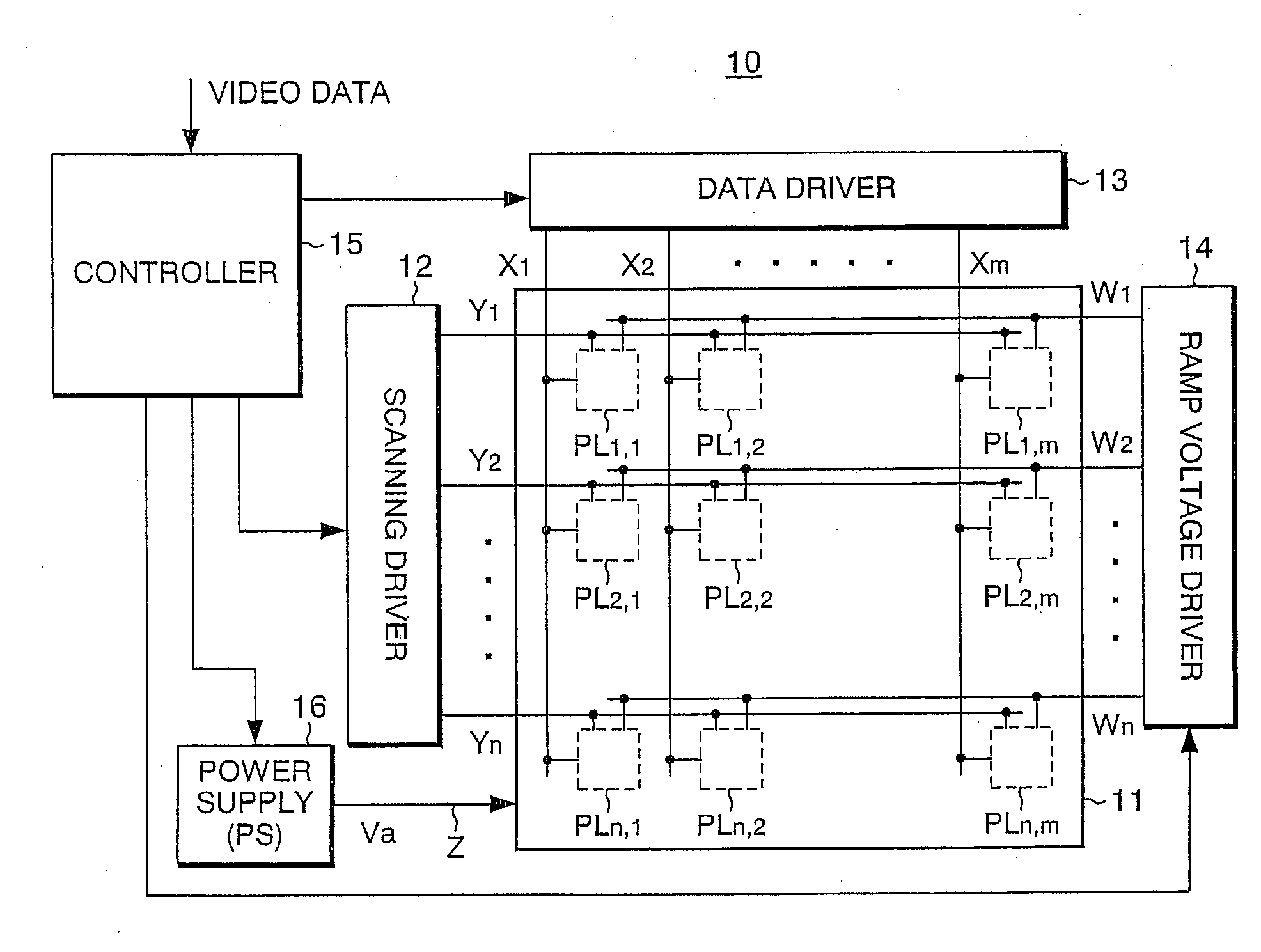
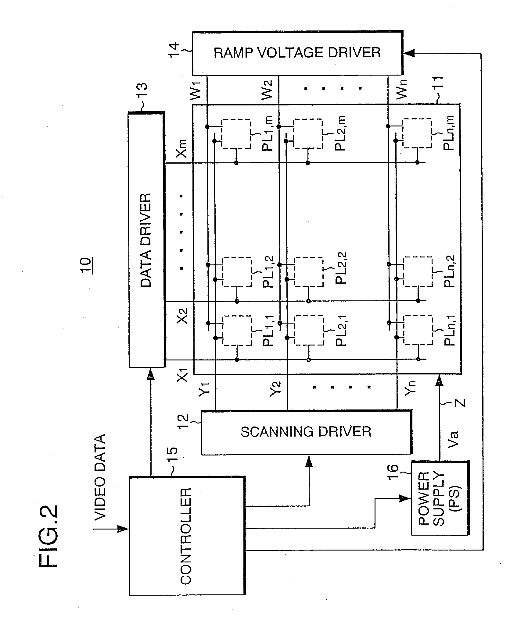
[0035]FIG. 2 illustrates a display apparatus 10 which uses an active matrix display panel according to a first embodiment of the present invention. The display apparatus 10 includes a display panel 11, a scanning driver 12, a data driver 13, a ramp voltage driver 14, a controller 15, and a light emission element driving power supply PS (hereinafter, simply referred to as power supply PS) 16.

[0036]The display panel 11 is an active matrix display panel constituted by m×n pixels (m, n: 2 or larger integers). The display panel 11 has a plurality of data lines X1 through Xm (Xi: i=1 through m) each of which is disposed in parallel with each other, a plurality of scanning lines Y1 through Yn (Yj: j=1 through n) each of which is disposed in parallel with each other, and a plurality of pixel units PL1,1 through PLn,m. The pixel units PL1,1 through PLn,m are disposed at the cross points of the data lines X1 through Xm and the scanning lines Y1 through Yn, and have the same structure. The pix...

second embodiment

[0066]FIG. 11 illustrates a structure of the display apparatus 10 according to a second embodiment of the present invention. The display apparatus 10 includes the display panel 11, the scanning driver 12, the data driver 13, the ramp voltage driver 14, the controller 15, and a capacitor power supply 16A.

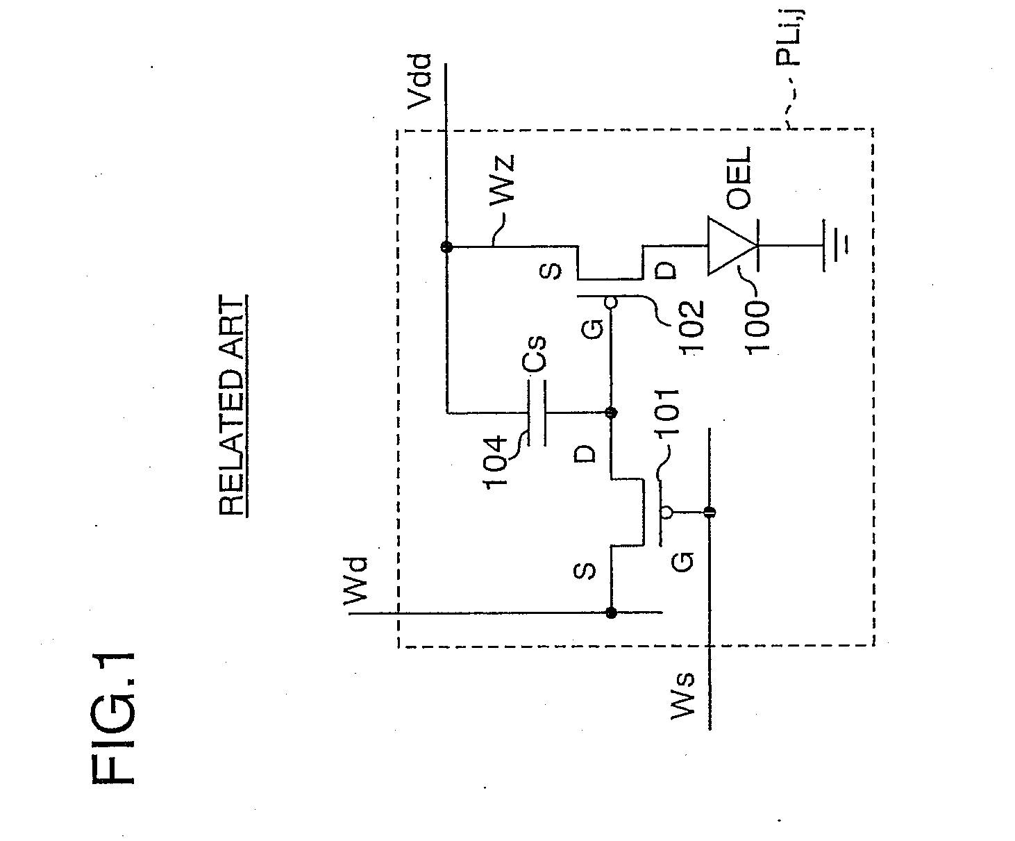
[0067]FIG. 12 shows the pixel unit PLj,i connected to the data line Xi (i=1, 2, through m) and the scanning line Yj (j=1, 2 through n) in the plurality of pixel units of the display panel 11. The pixel unit PLj,i has the TFTs (thin film transistors) 21 and 22 as selector transistor (Tr1) and driver transistor (Tr2), respectively, the data holding capacitor (Cs) 24, and the organic EL (electroluminescence) light emission element (OEL) 25 in the same manner as in the first embodiment.

[0068]In this embodiment, the second terminals (electrodes E2) of the capacitors (Cs) 24 of all the pixels in the display panel 11 are connected to a common connection line Z. The capacitor power supply 16...

third embodiment

[0077]FIG. 14 illustrates the pixel unit PLj,i connected to the data line Xi (i=1, 2, through m) and the scanning line Yj (j=1, 2 through n) in the plurality of pixel units of the display panel 11 according to a third embodiment of the present invention.

[0078]The analog driving system which writes analog data to pixels and modulates light emission luminance by an analog method for luminance control involves a current designation type which uses current for data designation as well as the voltage designation type discussed above which uses voltage for data designation. According to this analog driving system, variations in the characteristics of the TFTs, the organic EL elements and the like are the problems. For compensating for the variations in the element characteristics of the TFTs and the like, voltage program method and current program method are used in some cases. For example, current program type and voltage program type proposed by Sarnoff Corp. et al. and disclosed in Dig...


PUM


Abstract

A display includes connection lines each of which is provided for the corresponding scanning line of the display and is connected to a light emission element driving circuit, a ramp voltage generating section for generating ramp voltage for varying the control electrode voltage of each of the driver transistors relative to the voltage of the other electrode of the corresponding driver transistor to change the emission state of the corresponding light emission element, and a ramp voltage driver for supplying the ramp voltage to each of the connection lines provided for the corresponding scanning line in response to the scanning.

Description

BACKGROUND OF THE INVENTION[0001]1. Field of the Invention[0002]The present invention relates to a display apparatus including active elements for driving light emission elements such as EL (electroluminescent) elements and LEDs (light emission diodes) and its driving method, and more particularly to a display apparatus including thin film transistors (TFTs) as active elements and the driving method therefor.[0003]2. Description of the Related Art[0004]TFTs are widely used as active elements for driving an active matrix display such as an organic EL display and a liquid crystal display. FIG. 1 shows a pixel PLi,j in an example of an equivalent circuit of a driving circuit in an organic EL (organic electroluminescent) element (OEL) or an organic light emission diode (OLED) 100.[0005]As illustrated in FIG. 1, the equivalent circuit includes two p-channel TFTs 101 and 102 as active elements and a capacitor (Cs) 104. A scanning line Ws is connected to the gate of the selector TFT 101. A...

Claims


Application Information

Patent Timeline
Patent Type & Authority Applications(United States)
IPC IPC(8): G09G3/30
CPCG09G3/3258G09G2300/0842G09G2300/0861G09G2300/0866G09G2320/02G09G2310/0259G09G2310/0262G09G2310/066G09G2300/0876
Inventor ISHIZUKA, SHINICHI
Owner PIONEER CORP
Why Eureka
Try Eureka