
System and method for testing a packetized memory device

a packetized memory and test system technology, applied in the field of memory devices, can solve problems such as large, complex, and expensive standalone test units, errors that may occur during use go undetected, and the regular pattern of data stored in the array of memory cells does not accurately simulate patterns

Inactive Publication Date: 2009-07-02
MICRON TECH INC
View PDF8 Cites 20 Cited by
  • Summary
  • Abstract
  • Description
  • Claims
  • Application Information

AI Technical Summary

Problems solved by technology

They are generally relatively large, complex, and expensive standalone test units, and, in some cases, may be connected to several test heads to simultaneously test the memory devices on several load boards.
The primary reason why errors that may occur during use go undetected is that the regular pattern of data stored in the array of memory cells does not accurately simulate patterns of data that are stored in the memory array during use.
Unfortunately, conventional testers that may use an algorithmic pattern generator generate data only in conjunction with conventional memory commands and memory addresses of the type received by dynamic random access memory devices, static random access memory devices, flash memory devices, etc.
Unfortunately, testers that can generate and insert in the packets an algorithmically generated pattern of data have not been developed.
Therefore, the benefits of being able to store data generated by an algorithm pattern generator is not available to testers for testing packetized memory devices.

Method used


Image

  • System and method for testing a packetized memory device
  • System and method for testing a packetized memory device
  • System and method for testing a packetized memory device

Examples


Embodiment Construction

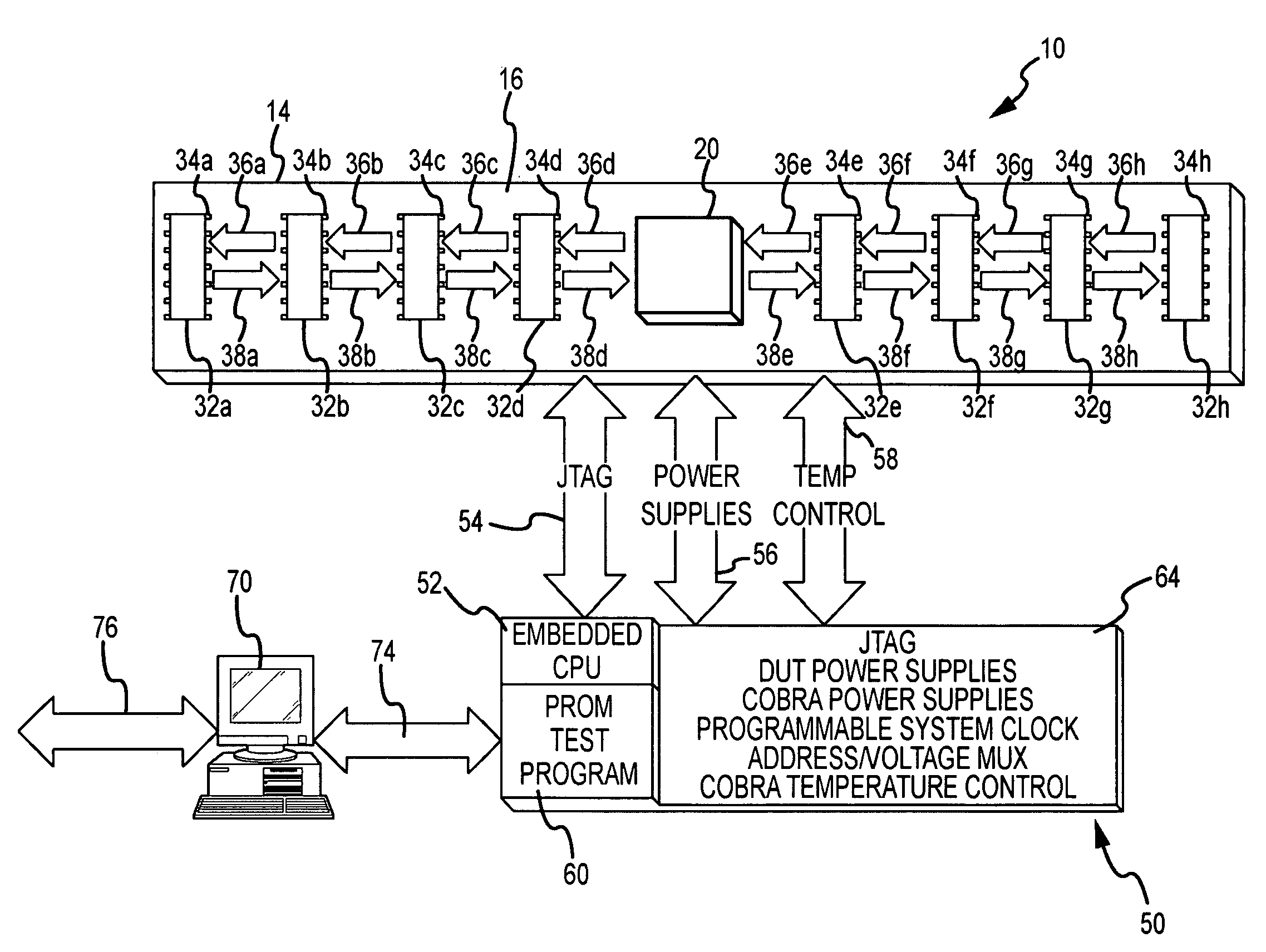
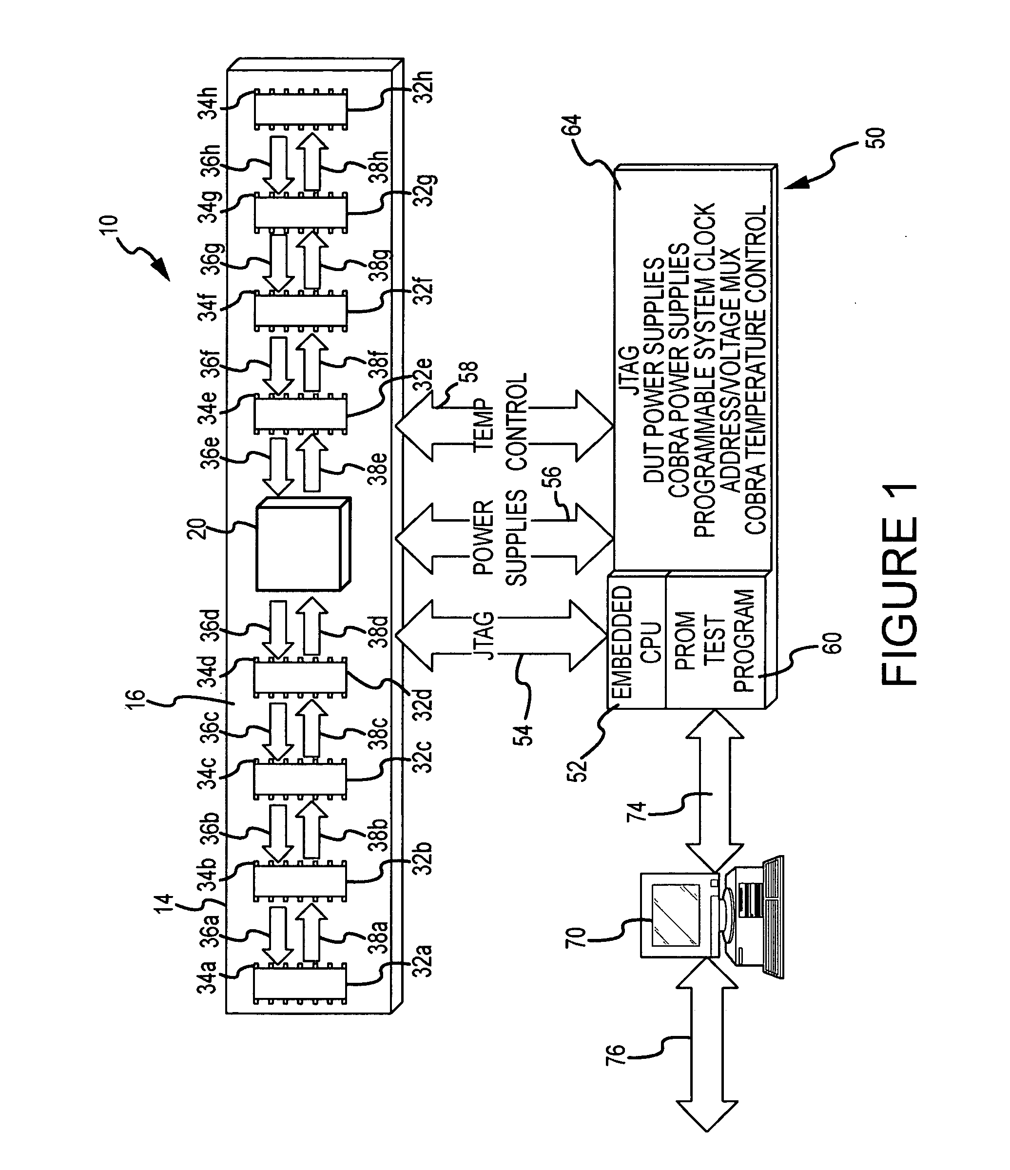
[0014]A test system 10 according to one embodiment of the invention is shown in FIG. 1. The test system 10 includes a load board 14 having an insulative substrate 16 on which is mounted a integrated test circuit 20 connected to eight memory devices 32a-h through respective sets of terminals 34a-h. Each of the terminals 34a-h may be formed by respective integrated circuit sockets. The memory devices 32a-h, which may be dynamic random access memory (“DRAM”) devices, are directly connected to the integrated test circuit 20 through respective high-speed downstream links 36a-h and respective high-speed upstream links 38a-h. The integrated test circuit 20 transmits packets containing a memory command digit, address digits and, in some cases, write data digits through the downstream links 36a-h to the respective memory devices 32a-h. The memory devices 32a-h may respond to the memory commands in the packet by writing a packet containing write data digits, e.g. bits, if the command is for a...


PUM


Abstract

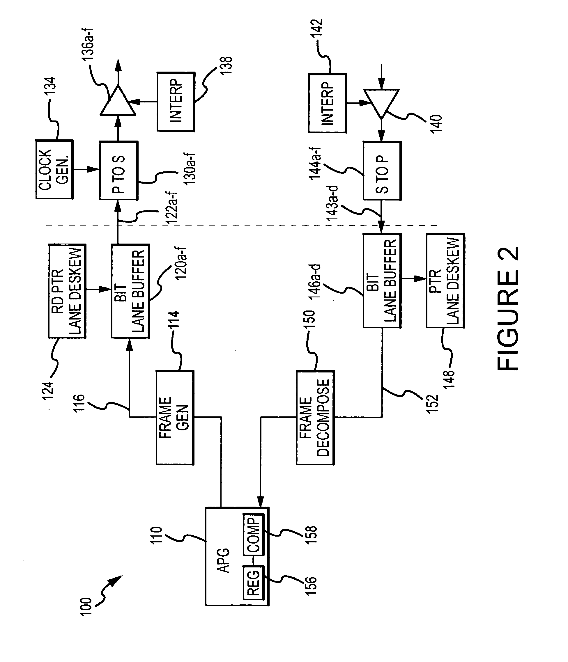
Integrated circuits, load boards and methods are disclosed, such as those associated with a memory testing system that includes an algorithmic pattern generator generating a pattern of command, address or write data digits according to an algorithm. In one such embodiment, the pattern of digits are applied to a frame generator that arranges the pattern of digits into a packet. The packet is then applied to a plurality of parallel-to-serial converters that convert the packet into a plurality of serial digits of a command / address packet or a write data packet, which are output through a plurality of bit lanes. The system might also include a plurality of serial-to-parallel converters receiving respective sets of digits of a read data packet through respective bit lanes. The read data packet is applied to a frame decomposer that extracts a pattern of read data digits from the packet. An error detecting circuit then determines if any of the received read data digits are erroneous.

Description

TECHNICAL FIELD[0001]This invention relates to memory devices, and, more particularly, in at least one embodiment, a memory device that receives packets comprising commands, addresses and write data.BACKGROUND OF THE INVENTION[0002]During the fabrication of memory devices, it is conventional to test the integrated circuits of the memory devices at several stages during the fabrication process. For example, the integrated circuits are normally connected to a tester with a probe card when the integrated circuits are still in wafer form. In a final test occurring after the integrated circuits have been diced from the wafer and packaged, the integrated circuits are placed into sockets on a load board. The load board is then placed on a test head, typically by a robotic handler. The test head makes electrical contact with conductors on the load board, and these conductors are connected to the integrated circuits. The test head is connected through a cable to a high-speed tester so that t...

Claims


Application Information

Patent Timeline
IPC IPC(8): G11C29/00
CPCG11C5/04G11C2029/5602G11C29/56
Inventor JEDDELOH, JOSEPH M.
Owner MICRON TECH INC
Learn More