Hyperspectral imaging device

a hyperspectral imaging and imaging device technology, applied in the field of imaging, can solve the problems of limiting system efficacy and a basic of the typical single crystal inorganic photodetectors

Active Publication Date: 2009-07-09
SAMSUNG ELECTRONICS CO LTD
View PDF68 Cites 103 Cited by
  • Summary
  • Abstract
  • Description
  • Claims
  • Application Information

AI Technical Summary

Problems solved by technology

Typical single-crystal inorganic photodetectors can suffer from a basic tradeoff of absorption cross-section for background noise.
The size and power-consumption attributes of equipment for cooling typical existing detectors have hindered the development of compact multi-color (“hyperspectral”) imaging system, and limit system efficacy by confining the existing detectors to large sized platforms.

Method used


Image

  • Hyperspectral imaging device
  • Hyperspectral imaging device
  • Hyperspectral imaging device

Examples


Embodiment Construction

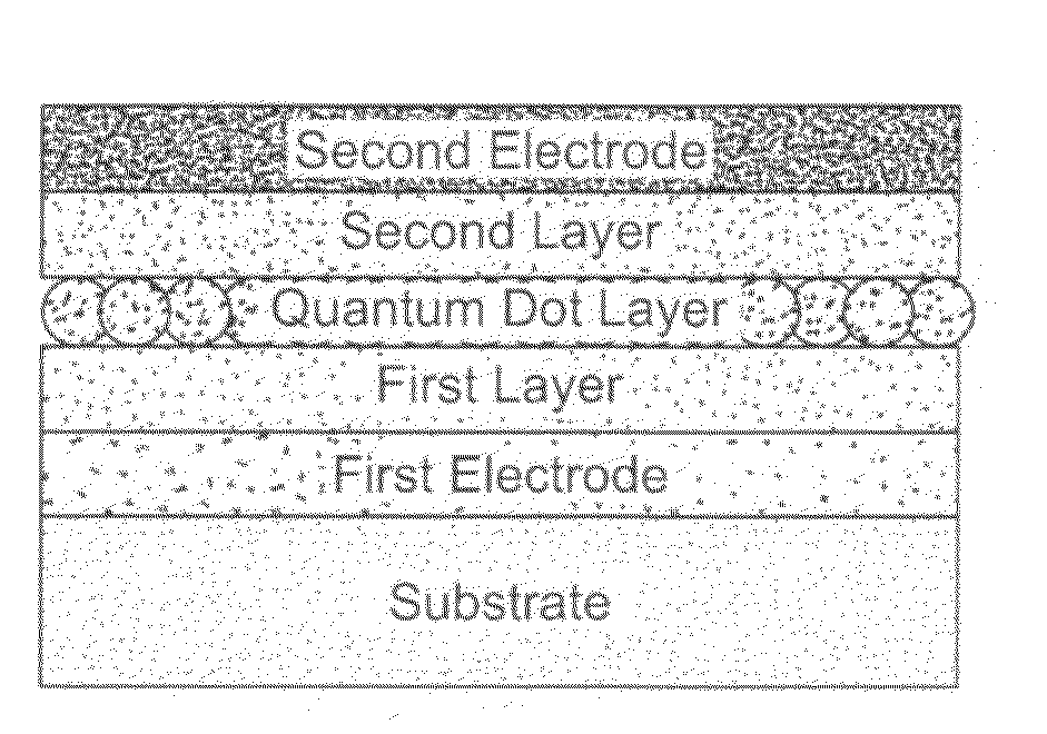
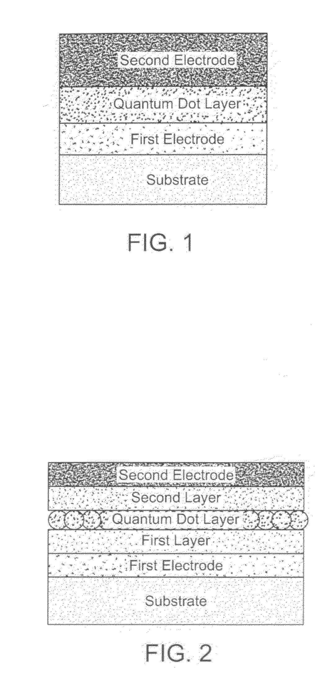
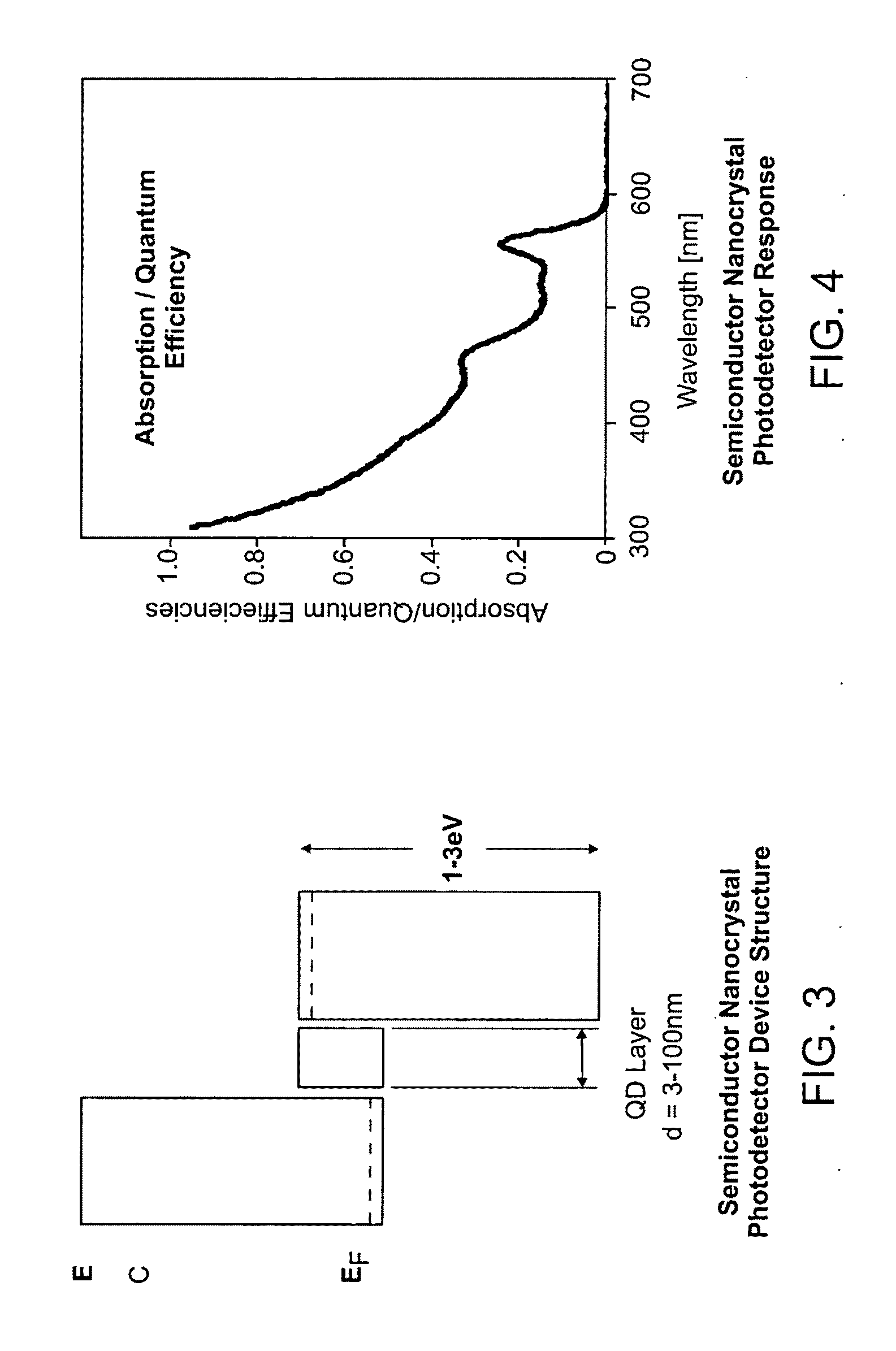
[0015]In accordance with one aspect of the invention, there is provided an hyperspectral imaging device comprising an array of semiconductor nanocrystals.

[0016]Preferably, at least a portion of the semiconductor nanocrystals are engineered to generate an electrical output in response to absorption of light having the wavelength to be detected, e.g., infrared light, visible, ultraviolet, etc.

[0017]The array of semiconductor nanocrystals is preferably disposed as a layer of semiconductor nanocrystals arranged in a pattern. The pattern can optionally including repeating sub-patterns. The pattern can include semiconductor nanocrystals arranged to detect a plurality of different wavelengths or wavelength bands, e.g., from 1 to 100, from 1 to 10, from 3 to 10, different wavelengths or wavelength bands.

[0018]In one example of a detailed aspect of the invention, the hyperspectral imaging device comprises two electrodes (e.g., anode and cathode) disposed on a substrate with an array of semic...


PUM


Abstract

An hyperspectral imaging device comprising semiconductor nanocrystals is provided.

Description

[0001]This application is a continuation of commonly owned PCT Application No. PCT / US2007 / 007424 filed 26 Mar. 2007, which was published in the English language as PCT Publication No. WO / 2007 / 112088 on 4 Oct. 2007. The PCT Application claims priority from commonly owned U.S. Application No. 60 / 785,786 filed 24 Mar. 2006. The disclosures of each of these applications are hereby incorporated herein by reference in their entireties.TECHNICAL FIELD OF THE INVENTION[0002]This invention relates generally to the field of imaging and more specifically to hyperspectral imaging.BACKGROUND OF THE INVENTION[0003]Typical single-crystal inorganic photodetectors can suffer from a basic tradeoff of absorption cross-section for background noise. For each unit thickness of absorbing bulk inorganic material, the possibility of a thermally generated electron-hole pairs increases. These thermally generated charge carriers contribute to the dark current of a photodetector device, and thus require the dev...

Claims


Application Information

Patent Timeline
Patent Type & Authority Applications(United States)
IPC IPC(8): H01L31/0224
CPCG01J3/2803H01L31/0352G01J3/2823
Inventor COE-SULLIVAN, SETHMOELLER, GREGORY V.
Owner SAMSUNG ELECTRONICS CO LTD
Why Eureka
Try Eureka