
Color converting material composition and color converting medium including same

a technology of color converting material and composition, which is applied in the direction of luminescent compositions, discharge tubes/lamp details, discharge tubes luminescent screens, etc., can solve the problems of deteriorating purity of displayed light, fluorescent semiconductor nanocrystals that cannot absorb organic el elements in sufficient quantities, and deteriorating purity of converted light. , to achieve the effect of reducing mechanical stability of the emitting apparatus, reducing conversion capability and reducing light outcoupling efficiency

Inactive Publication Date: 2009-01-22
IDEMITSU KOSAN CO LTD
View PDF5 Cites 73 Cited by
  • Summary
  • Abstract
  • Description
  • Claims
  • Application Information

AI Technical Summary

Benefits of technology

[0081]Since both the color converting film and the color converting multi-layer stack of the invention contain both the fluorescent semiconductor nanocrystal and the organic fluorescent dye, the above-mentioned advantageous effects of the invention can be obtained.
[0082]The mixing ratio of the fluorescent semiconductor nanocrystal to the light-transmissible matrix (fluorescent semiconductor nanocrystal / light-transmissible matrix: weight ratio) in the first color converting film is preferably 1 / 20 to 4 / 6, and still more preferably 1 / 9 to 3 / 7, although the mixing ratio varies depending on the specific gravity and the particle size of the fluorescent semiconductor nanocrystal. If the mixing ratio is less than 1 / 20, the fluorescent semiconductor nanocrystal may not sufficiently absorb the light emitted from the emitting device, whereby conversion capability may be lowered or chromaticity after conversion may deteriorate. If the thickness of the converting layer is increased in order to allow the converting layer to absorb the light emitted from the emitting device, the mechanical stability of the emitting apparatus may be decreased due to thermal stress or the like, or it may become difficult to make the color conversion substrate flat. This may result in improper distances between the emitting devices and the color conversion substrate, whereby the visibility (e.g. viewing angle characteristics) of the emitting apparatus may be adversely affected.
[0083]If the mixing ratio exceeds 4 / 6, it may become difficult to stably disperse the fluorescent semiconductor nanocrystal by controlling the particle size. Further the light outcoupling efficiency may be decreased due to an increase in the refractive index, or it may become difficult to form a pattern.
[0084]The mixing ratio of the organic fluorescent dye and the light-transmissible matrix (organic fluorescent dye / light-transmissible matrix:weight ratio) in the second color converting film is preferably 1 / 10000 to 1 / 20, more preferably 1 / 1000 to 1 / 30, although the mixing ratio depends on the kind of the organic fluorescent dye. If the mixing ratio is smaller than 1 / 10000, conversion capability may be lowered or chromaticity after conversion may deteriorate. If the mixing ratio exceeds 1 / 20, the organic fluorescent dyes may contact with other to cause concentration quenching.
[0085]The thickness of the color converting film of the invention is preferably 1 μm to 100 μm, particularly preferably 1 μm to 30 μm.
[0086]The thickness of the first color converting film of the color converting multi-layer stack is preferably 1 μm to 100 μm, particularly preferably 1 μm to 30 μm.

Problems solved by technology

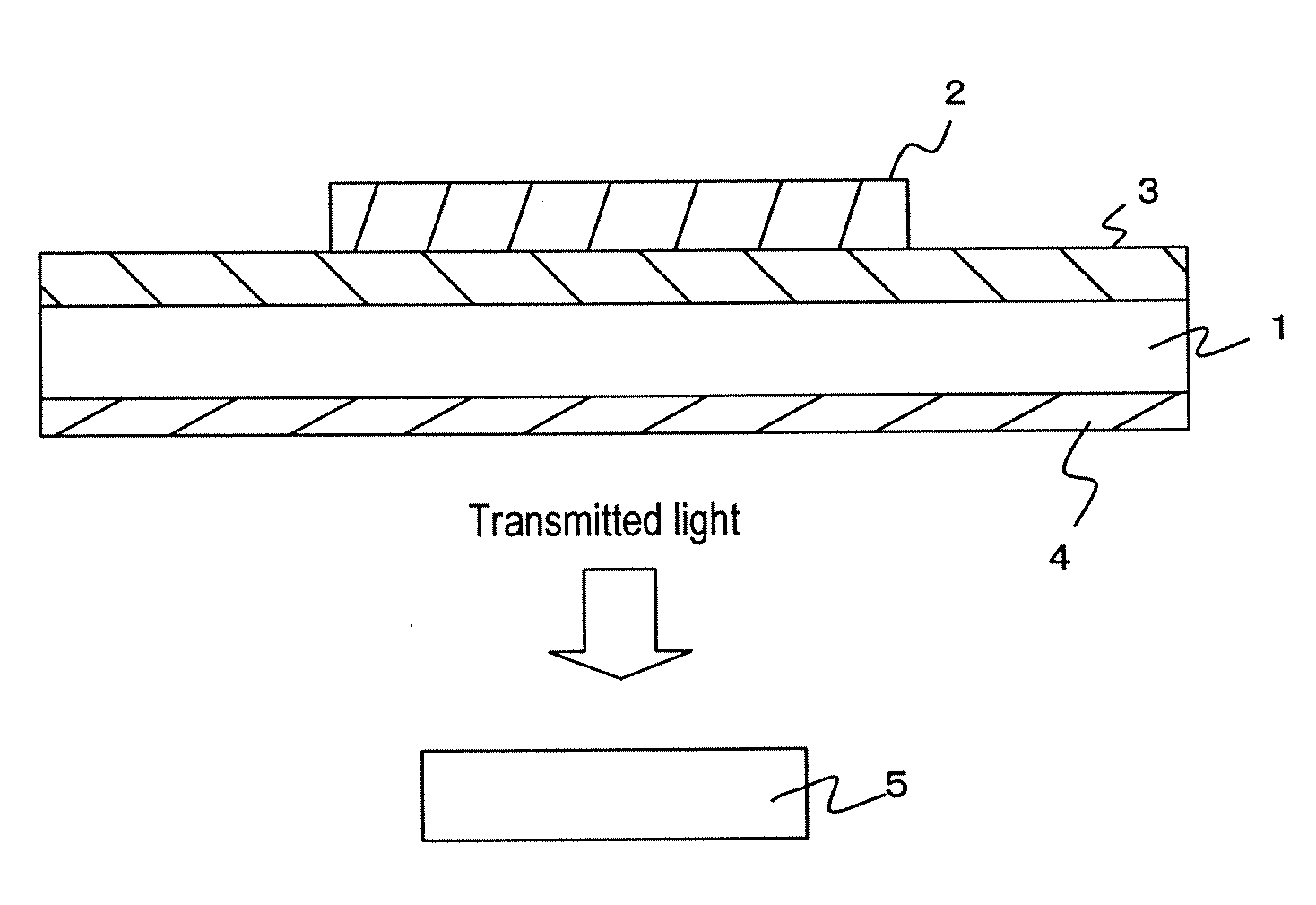
However, when an organic electroluminescent device (hereinafter “electroluminescent” will be abbreviated as “EL”) or the like is used as a light source, a color converting substrate using a semiconductor nanocrystal suffers deteriorated purity of converted light.
Therefore, when an organic EL element is combined with a color converting substrate containing a fluorescent semiconductor nanocrystal, the fluorescent semiconductor nanocrystal cannot sufficiently absorb emission from the organic EL element.
As a result, the amount of leaked light which passes through the color converting substrate without being converted increases, causing the purity of displayed light to deteriorate.
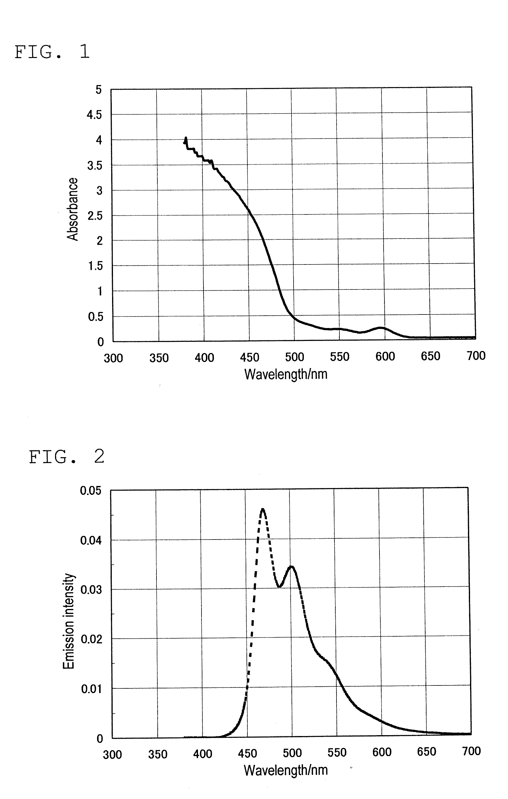
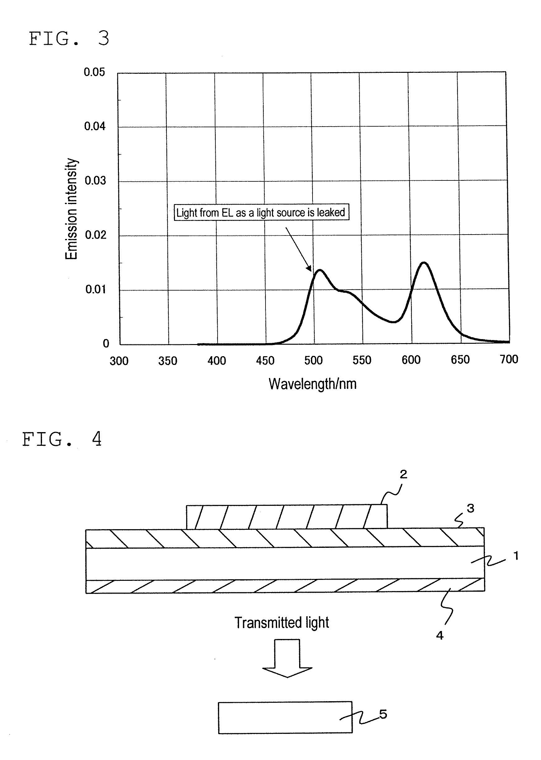
However, if the amount of unnecessary light components is extremely large, as shown in FIG. 3, color purity cannot be corrected to a sufficient level.

Method used


Image

  • Color converting material composition and color converting medium including same
  • Color converting material composition and color converting medium including same
  • Color converting material composition and color converting medium including same

Examples


synthesis example 1

[0101](1) 0.5 g of cadmium acetate dihydrate and 1.6 g of tetradecylphosphonic acid (TDPA) were added to 5 ml of trioctylphosphine (TOP). The resulting solution was heated to 230° C. and stirred for one hour in a nitrogen atmosphere. After cooling the solution to 60° C., 2 ml of a TOP solution containing 0.2 g of selenium was added to the solution to obtain a raw material solution.

[0102]10 g of trioctylphosphine oxide (TOPO) was placed in a three-necked flask and dried at 195° C. for one hour under vacuum. After setting the pressure inside the flask at atmospheric pressure using nitrogen gas, the TOPO was heated to 270° C. in a nitrogen atmosphere. 1.5 ml of the above raw material solution was added to the TOPO while stirring the system to allow a reaction to initiate.

[0103]The reaction was continued while confirming the growth of the nanocrystal. When the particle size of the nanocrystal became a desired size, the reaction solution was cooled to 60° C. to terminate the reaction.

[01...

synthesis example 2

Synthesis of ZnTe / ZnSe Semiconductor Nanocrystal

[0107]The ZnTe / ZnSe semiconductor nanocrystal was synthesized with reference to JP-T-2003-505330. Specifically, TOPO (40 g) and myristic acid (0.1 g) were placed in a four-necked flask and dried at 180° C. for two hours under reduced pressure. After setting the pressure inside the flask at atmospheric pressure using nitrogen gas, a zinc acetate / TOP solution which had been prepared separately (8.5 ml, containing 0.3 g of zinc acetate) and heated to 100° C. was added. The resulting mixture was heated to 330° C.

[0108]A tellurium / hexapropylphosphorous triamide / TOP solution (1.5 ml, containing 0.3 g of tellurium) was poured into the above four-necked flask, and the resulting mixture was stirred at 280° C. for 2 hours.

[0109]The reaction solution was cooled to 150° C. A diethyl zinc / bis(trimethylsilyl)selenide / TOP solution (10 ml, containing 0.14 g of diethyl zinc, 0.25 g of bis(trimethylsilyl)selenide)) was added dropwise over a period of on...

synthesis example 3

Synthesis of Inp / Znse Semiconductor Nanocrystal

[0112]TOPO (4 g) and TOP (36 g) was placed in a four-necked flask and dried at 100° C. for two hours under reduced pressure. After setting the pressure inside the flask at atmospheric pressure using nitrogen gas, an indium acetate / TOPO / TOP solution which had been prepared separately (6.4 ml, containing 0.34 g of indium acetate, the TOPO / TOP amount ratio was the same as in the flask) and heated to 100° C. was added. The resulting mixture was heated to 310° C.

[0113]A hexapropylphosphorous triamide / TOP solution (4.4 ml, containing 0.32 g of hexaethylphosphorous triamide) was added to the above four-necked flask, and the resulting mixture was stirred at 310° C. for 2 hours.

[0114]The reaction solution was cooled to 150° C. A diethyl zinc / bis(trimethylsilyl)selenide / TOP solution (10 ml, containing 0.14 g of diethyl zinc, 0.25 g of bis(trimethylsilyl)selenide)) was added dropwise over a period of one hour. After completion of the dropwise addi...


PUM


Abstract

A color converting material composition including: a light-transmissible matrix; a fluorescent semiconductor nanocrystal which absorbs at least light in a first wavelength region; and an organic fluorescent dye which absorbs at least light in a second wavelength region.

Description

TECHNICAL FIELD[0001]The invention relates to a color converting material composition and a color converting medium (color converting film, color converting multi-layer stack, color converting substrate, emitting device) containing the same.BACKGROUND[0002]A color converting substrate utilizing a color converting material composition which converts the wavelength of light emitted from a light source using a fluorescent material has been applied in various fields including the electronic display field. An emitting apparatus utilizing a color converting substrate can emit light of a plurality of colors from a monochromic light source (blue light, for example).[0003]An organic fluorescent material and an inorganic fluorescent material have been used as the fluorescent material used for the color converting material composition.[0004]A fluorescent dye and a fluorescent pigment have been studied as the organic fluorescent material. As the inorganic fluorescent material, a material of a m...

Claims


Application Information

Patent Timeline
IPC IPC(8): H01J1/62
CPCC09K11/06C09K2211/1029H05B33/14H01L51/5036H01L51/0053Y02E10/549H10K85/621H10K50/125H01L2924/1307H10K77/10
Inventor HACHIYA, SATOSHIKATANO, JUNICHI
Owner IDEMITSU KOSAN CO LTD
Learn More