Semiconductor-nanocrystal/conjugated polymer thin films

a technology of monocrystalline crystals and polymer thin films, which is applied in the direction of organic semiconductor devices, crystal growth processes, polycrystalline material growth, etc., can solve the problems of high cost of manufacturing solar cells of the prior art, limiting their widespread use as a source of power, and increasing manufacturing costs, so as to achieve high loading amounts

Active Publication Date: 2005-06-23
RGT UNIV OF CALIFORNIA
View PDF38 Cites 77 Cited by
  • Summary
  • Abstract
  • Description
  • Claims
  • Application Information

AI Technical Summary

Problems solved by technology

Despite these impressive efficiencies, the high cost of manufacturing solar cells of the prior art limits their widespread use as a source of power.
The gain in performance results in increased manufacturing costs, which stem from the multiplication of the number of fabrication steps.
Another problem with the solar devices of the prior art is the high cost of manufacturing materials.
Because solar cells are large area devices, such material costs hinder the production of inexpensive cells.
Further improvements in efficiencies are limited by the poor electron transport properties of C60, which is characterized by hopping, and the low overlap between the device absorption and the solar emission spectrum, Greenham. N. C. et al., Phys Rev.

Method used


Image

  • Semiconductor-nanocrystal/conjugated polymer thin films
  • Semiconductor-nanocrystal/conjugated polymer thin films
  • Semiconductor-nanocrystal/conjugated polymer thin films

Examples


example 1

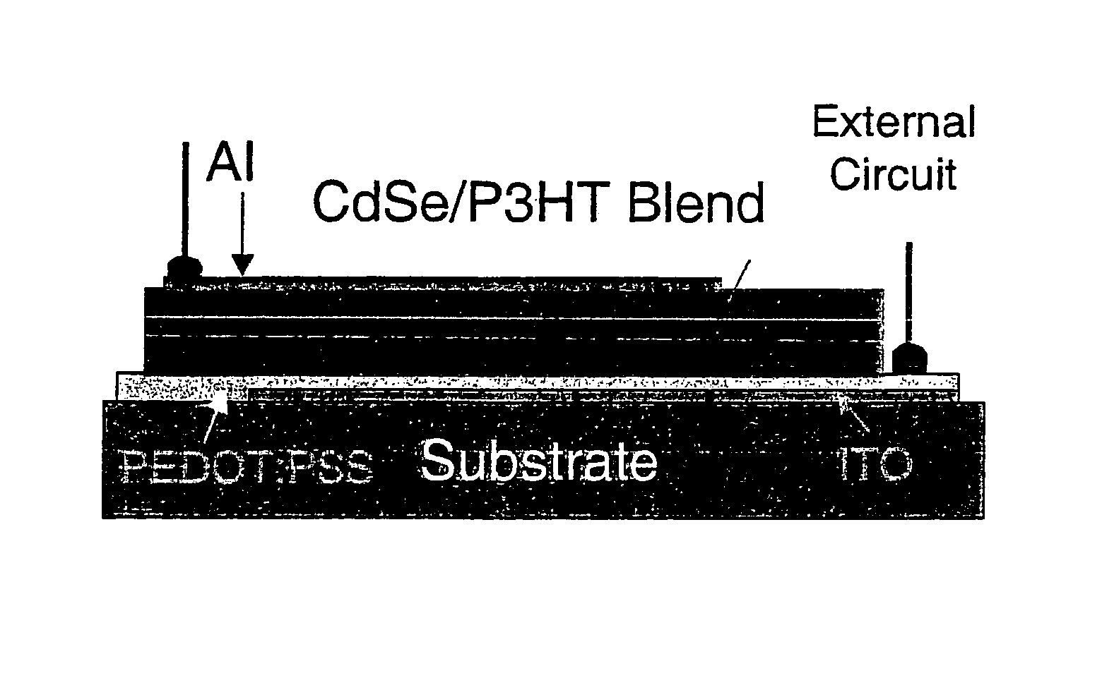
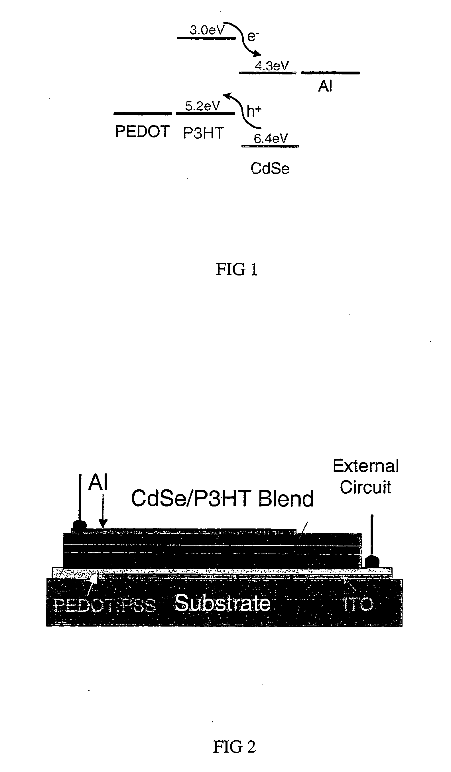
[0125] According to one embodiment of the invention, photovoltaic devices were fabricated from spin casting a solution of CdSe nanocrystals and P3HT in a pyridine-chloroform solvent mixture onto an ITO coated glass substrate under inert atmosphere, pumping for 12 hours under −6 mbar and evaporating aluminum on top to obtain the structure depicted in FIG. 2.

example 2

[0126] a. Nanocrystal Synthesis: According to another embodiment of the invention long CdSe nanorods in P3HT (90 wt % CdSe) were synthesized as follows: Cd stock: 0.161 g of dimethylcadmium was dissolved in 0.34 g of trioctylphosphine (TOP). Se stock: 0.2 g of Se in 2.367 g of TOP was dissolved. In a three neck flask, 3.536 g of trioctylphosphine oxide (TOPO), 0.187 g of hexylphosphonic acid (HPA), and 0.357 g tetradecylphosphonic acid (TDPA) were mixed. This mixture was heated and degassed under argon to 360C. Cd stock was slowly injected, then the temperature was lowered to 330C the Se stock was rapidly injected. The reaction was allowed to proceed at 290C for 18 minutes then the heat was removed. At 40C, about 15 mL of methanol was added to the flask. The mixture was centrifuged and the supernatant was discarded. 8 mL of methanol was added, vortex, then again centrifuge, discarding the supernatant.

[0127] b. Substrate Preparation: Wash indium tin oxide (ITO) on glass substrates b...

example 3

CdTe Tetrapods in P3HT

[0131] CdTe tetrapod nanocrystals having a core and 4 arms of approximately 80 nm in length were synthesized then washed with several dissolution / precipitation steps in tetrahydrofuran (THF) and ethylacetate.

[0132] The nanocrystals were then codissolved in solvent chloroform with the ligand phenylphosphonic acid and heated at around 100C for several hours.

[0133] The nanocrystals were then precipatated with methanol and redissolved in chloroform.

[0134] The nanocrystal solution was mixed with a P3HT solution as described in example 2 and spin cast to create thin films.

[0135] Substrates and electrodes were processed as in example 2. The EQE value for this sample was less than 10%.


PUM

PropertyMeasurementUnit
thicknessaaaaaaaaaa
thicknessaaaaaaaaaa
aspect ratioaaaaaaaaaa

Abstract

The invention described herein provides for thin films and methods of making comprising inorganic semiconductor-nanocrystals dispersed in semiconducting-polymers in high loading amounts. The invention also describes photovoltaic devices incorporating the thin films

Description

CROSS-REFERENCES TO RELATED APPLICATIONS [0001] This application is a non-provisional application based on U.S. Provisional Patent Application No. 60 / 365,401, filed Mar. 19, 2002; No. 60 / 381,660, filed May 17, 2002 and No. 60 / 381,667, also filed on May 17, 2002. These U.S. Provisional Patent Applications are herein incorporated by reference in their entirety for all purposes. Copending U.S. patent applications are U.S. Ser. No. 10 / 301,510, filed Nov. 20, 2002, which claims priority to U.S. Ser. No. 60 / 335,435, filed Nov. 30, 2001; and U.S. Ser. No. 10 / 280,135, which claims priority to U.S. Ser. No. 60 / 395,064, filed Jul. 12, 2002 and No. 60 / 346,253, filed Oct. 24, 2001. The contents of both utility applications and all provisional applications are incorporated by reference in their entirety for all purposes.STATEMENT AS TO RIGHTS TO INVENTIONS MADE UNDER FEDERALLY SPONSORED RESEARCH OR DEVELOPMENT [0002] The invention described and claimed herein was made in part utilizing funds sup...

Claims


Application Information

Patent Timeline
Patent Type & Authority Applications(United States)
IPC IPC(8): C09K19/02C09K19/52C30B7/00C30B29/40C30B29/48C30B29/60H01L31/0384H01L51/00H01L51/30H01L51/42
CPCB82Y20/00Y10S117/903C09K19/02C09K19/52C30B29/40C30B29/48C30B29/605H01L31/0384H01L51/0036H01L51/0037H01L51/426H01L51/4266H01L2251/308C30B7/005Y02E10/549B82Y30/00H10K85/1135H10K85/113H10K30/352H10K30/35H10K2102/103
Inventor ALIVISATOS, A. PAULDITTMER, JANKE J.HUYNH, WENDY U.MILLIRON, DELIA
Owner RGT UNIV OF CALIFORNIA
Why Eureka
Try Eureka