Method for forming nanostructure having high aspect ratio and method for forming nanopattern using the same

a nanostructure and aspect ratio technology, applied in the field of forming nanostructures with high aspect ratios, can solve the problems of difficult and complicated process, and difficult to form patterns using engraving molds or molds, etc., to achieve high aspect ratio, simple and economical process, and high aspect ratio

Inactive Publication Date: 2008-01-03
SEOUL NAT UNIV R&DB FOUND
View PDF21 Cites 77 Cited by
  • Summary
  • Abstract
  • Description
  • Claims
  • Application Information

AI Technical Summary

Benefits of technology

[0014] It is one object of the present invention to provide a method of forming a structure having a nano-sized diameter and a high aspect ratio through a simple and economical process.
[0015] It is another object of the present invention to provide a method of forming a nanopattern using the method of forming a structure having a nano-sized diameter and a high aspect ratio.
[0019] The method according to the present invention forms a nanostructure having a high aspect ratio through a simple process. Thus, the method according to the present invention can be applied to diverse fields requiring the formation of a nanostructure having a high aspect ratio and improve the processing and economical efficiencies of the fields.

Problems solved by technology

However, since the method requires a mold of a high hardness and high pressure, it is difficult to form patterns by using an engraved mold or molds having patterns of diverse sizes and to form a pattern in a wide area.
However, since the method should use a chemical material, i.e., PDMS, there is a shortcoming that it cannot form a structure having a high aspect ratio.
However, since multiple layers of molds should be arranged precisely to form a reliable structure having a high aspect ratio, the process is difficult and complicated.
Most of them have an advantage that, since an elastic PDMS mold having a low hardness is used, a three-dimensional microstructure can be formed in a wide area, but they have a conclusive limitation that they can hardly form a nano-sized structure.
Although the method has an advantage that delicate structure can be formed, it has a shortcoming that the process is remarkably slow because every single structure should be formed with the probe and, accordingly, it can be hardly applied to a wide area.
Therefore, they have shortcomings that they should use multiple sheets of masks, that the process is complicated and takes long time, and that they require a high amount of costs.

Method used


Image

  • Method for forming nanostructure having high aspect ratio and method for forming nanopattern using the same
  • Method for forming nanostructure having high aspect ratio and method for forming nanopattern using the same
  • Method for forming nanostructure having high aspect ratio and method for forming nanopattern using the same

Examples


embodiment

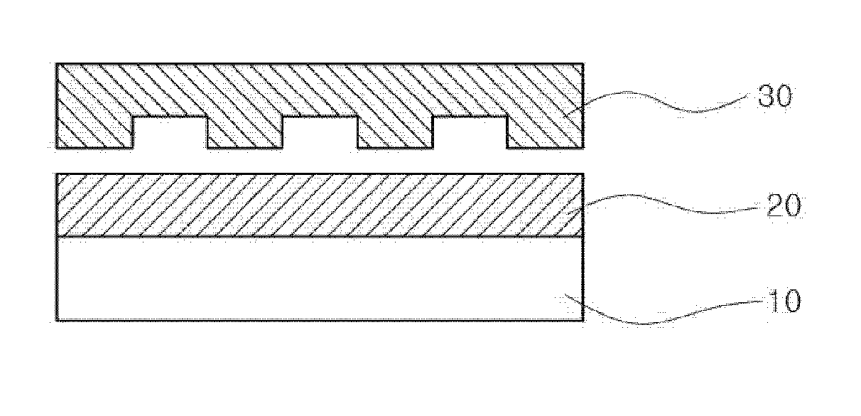
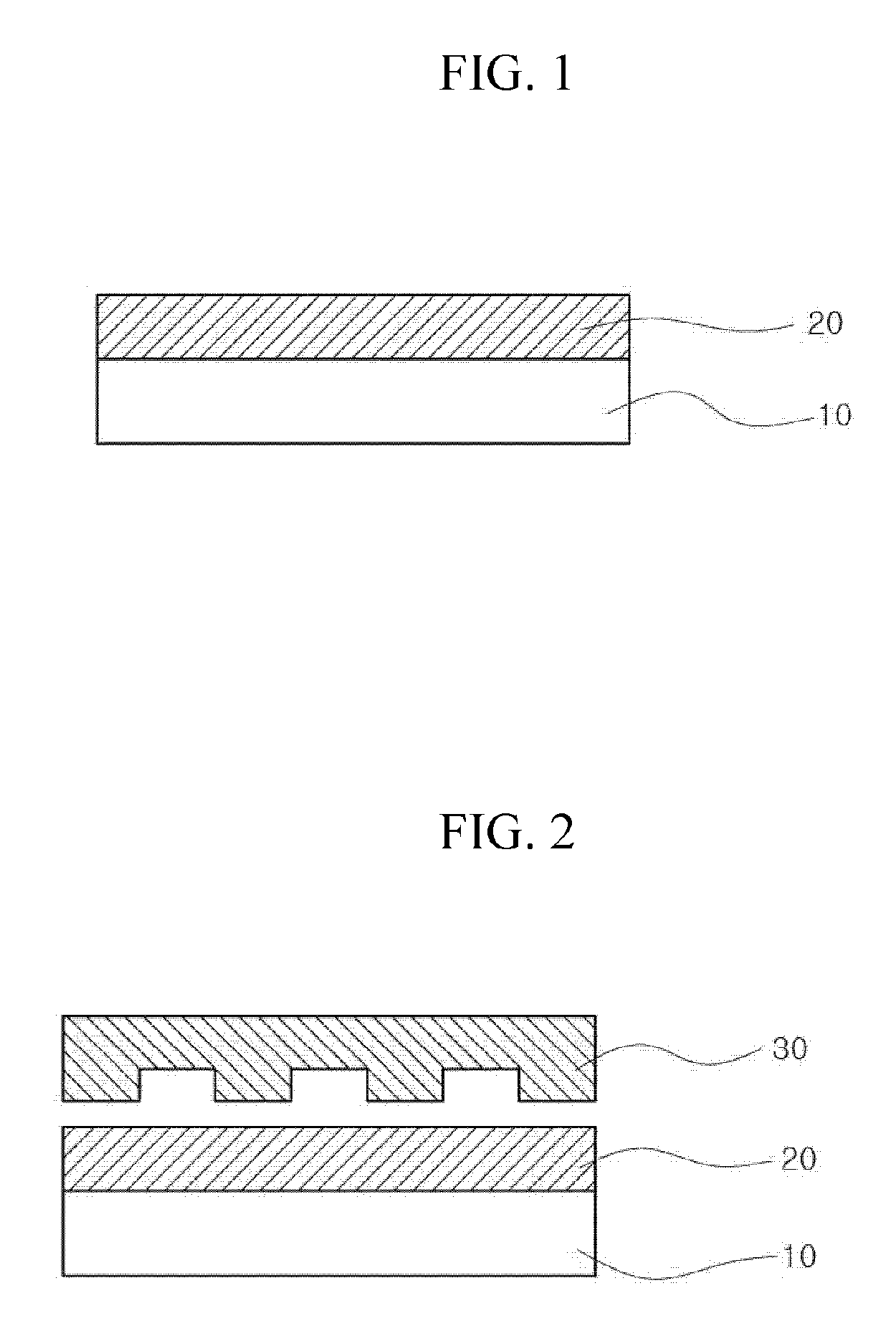
[0063] Operation S10: Formation of Polymer Thin Film on Substrate

[0064] First, a silicon substrate was washed by ultrasonic waves in an ultrasonic bath containing trichloroethylene (TCE) solution for about five minutes. Then, the silicon substrate was put in an ultrasonic bath containing methanol solution and washed by ultrasonic waves for about five minutes. The silicon substrate was taken out of the ultrasonic bath and rinsed with distilled water. Subsequently, the substrate was coated with a polymer thin film by using 30 wt % polystyrene dissolved in toluene. The coating was carried out in a spin coating method at 3,000 rpm.

[0065] Operations S20 and S30: Contact With Mold And Formation of Polymer Pattern

[0066] The polymer thin film was brought to a contact with a polyurethane mold having a desired pattern formed therein. The contact was performed evenly in such a manner that the contacting surface does not come off. The polymer thin film and the mold were maintained to contact...


PUM

PropertyMeasurementUnit
pressureaaaaaaaaaa
aspect ratioaaaaaaaaaa

Abstract

Provided is a method of forming a nanostructure having a nano-sized diameter and a high aspect ratio through a simple and economical process. To form the nanostructure, a polymer thin film is formed on a substrate and a mold is brought to contact the polymer thin film. Then, a polymer patterning is formed to contact the background surface of an engraved part of the mold, and then the polymer pattern is extended out by removing the mold out of the polymer thin film. The nanostructure forming method of the present research can reproduce diverse cilia optimized in the natural world. Also, it can be used to develop new materials with an ultra-hydrophobic property or a high adhesiveness. Further, it can be applied to a nanopattern forming process for miniaturizing electronic devices and to various ultra-precise industrial technologies together with carbon nanotube, which stands in the highlight recently.

Description

BACKGROUND OF THE INVENTION [0001] 1. Field of the Invention [0002] The present invention relates to a method of forming a nanostructure having a high aspect ratio and a method of forming a nanopattern by using the same; and more particularly, to a high-aspect ratio nanostructure forming method with simplified processing and excellent economical efficiency, and a nanopattern forming method using the same. [0003] 2. Description of the Related Art [0004] The major trend in manufacturing of industrial parts since 1980s has been miniaturization, and this calls for the development of nano-sized structures, which will be referred to as nanostructures hereinafter. To meet the demand, there are many techniques introduced for easily and economically forming reliable nanostructures. [0005] One of the representative methods for forming a nanostructure is nanoimprint lithography, which is disclosed in U.S. Pat. No. 5,772,905. To describe the technique in detail, a hard mold having a nano-sized ...

Claims


Application Information

Patent Timeline
Patent Type & Authority Applications(United States)
IPC IPC(8): C23F1/00B44C1/22
CPCB82Y10/00B82Y40/00H01L21/0337G03F7/0002C03C17/3405B82B3/00B82B1/00B29C59/02B29C39/10
Inventor SUH, KAHP-YANGJEONG, HOON-EUI
Owner SEOUL NAT UNIV R&DB FOUND
Why Eureka
Try Eureka