Flexible force or pressure sensor array using semiconductor strain gauge, fabrication method thereof and measurement method thereof

a technology of flexible force or pressure sensor array and strain gauge, which is applied in the direction of force measurement, measurement devices, instruments, etc., can solve the problems of reducing sensitivity, limiting quantitatively measuring the distribution of force or pressure, and limited application of flexible and bendable force or pressure sensing arrays, etc., to achieve increased strain, sensor structure is physically robust, and sensor structure. robust

Active Publication Date: 2011-09-22
KOREA RES INST OF STANDARDS & SCI
View PDF4 Cites 80 Cited by
  • Summary
  • Abstract
  • Description
  • Claims
  • Application Information

AI Technical Summary

Benefits of technology

[0012]Therefore, according to an embodiment of the present invention described above, first, the sensor structure of the present invention is simple and robust. That is, a structure having a wide membrane is generally adopted as a sensing unit of a sensor in order to increase the strain, and since a ductile polymer substrate itself functions as a sensing unit in the present invention, the sensor structure is physically robust. In addition, since a polymer is generally a chemical inert material, the sensor structure of the present invention is chemically stable. Second, since a semiconductor strain gauge is fabricated by injecting impurities such as Boron (B) into non-organic silicon and forming piezo resistance, sensitivity of signals is extraordinarily superior. Furthermore, repeatability and reproducibility of the signal output from the semiconductor strain gauge is superior compared with a method using force sensitive resistors.
[0013]Third, since changes of resistance in each element configuring a semiconductor strain gauge array pattern are processed using a CMOS circuit signal processing method, it is possible to further correctly measure resistance and voltage values, simplify the configuration of a circuit, and preprocess a signal within a tactile sensor. Fourth, the force sensor array of the present invention may have both flexibility and elasticity. Since the substrate itself is a kind of a polymer material, the substrate can be bent or expanded. Although non-organic silicon, which is a material of the semiconductor strain gauge and the CMOS circuit, is easily broken and solid, mechanical flexibility can be secured if it is fabricated extremely thin. In addition, even elasticity can be provided if it is fabricated in a corrugated structure.

Problems solved by technology

However, this method is disadvantageous in that since a gauge factor is lower than that of a semiconductor strain gauge as much as 50 to 100 times, sensitivity is lowered as much.
However, due to lack of flexibility and problems of conventional fabricating processes that cannot be done together with like a polymer-based fabricating process, its application to a flexible and bendable force or pressure sensing array is limited.
However, since the characteristics of the sensor array depend on conductivity of the metal particles scattered in the base material, repeatability and restorability are significantly lowered, and thus there is a limit in quantitatively measuring distribution of force or pressure.
However, since a complex electronic circuit is needed in order to implement the zero potential method, it is difficult to integrate the electronic circuit with a small tactile sensor.
Accordingly, as the tactile sensor is getting smaller and the number of arrays is increased, the number of signal lines is increased and the tactile sensor becomes further vulnerable to noises if the entire signal processing is performed outside the tactile sensor.

Method used


Image

  • Flexible force or pressure sensor array using semiconductor strain gauge, fabrication method thereof and measurement method thereof
  • Flexible force or pressure sensor array using semiconductor strain gauge, fabrication method thereof and measurement method thereof
  • Flexible force or pressure sensor array using semiconductor strain gauge, fabrication method thereof and measurement method thereof

Examples


Embodiment Construction

[0027]

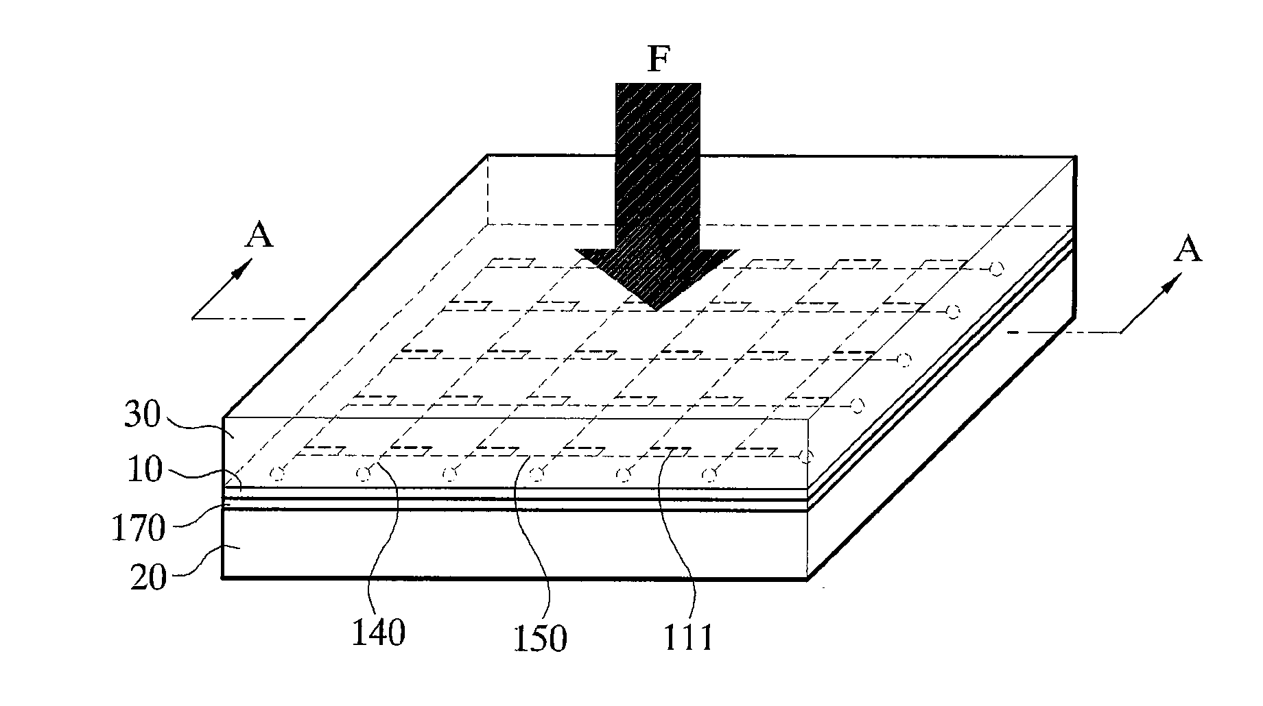
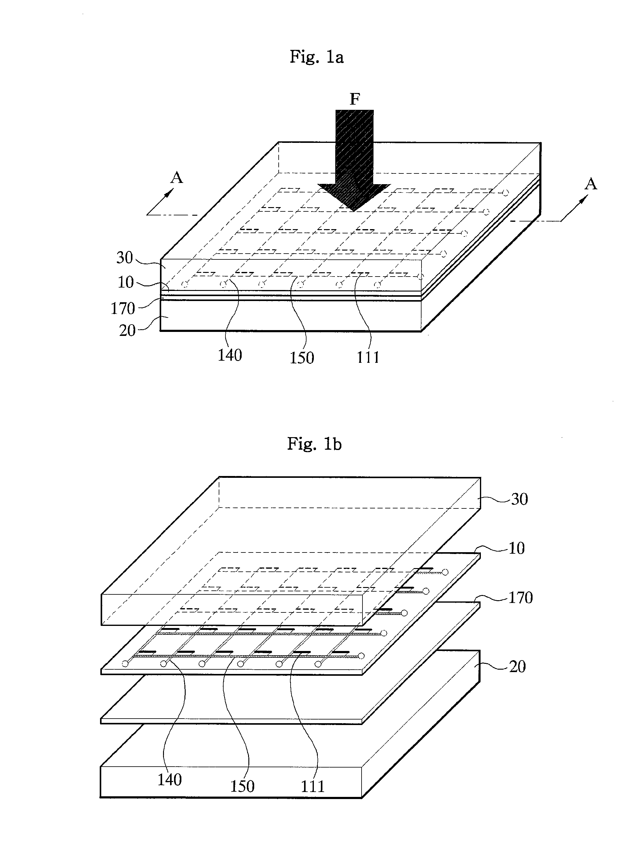
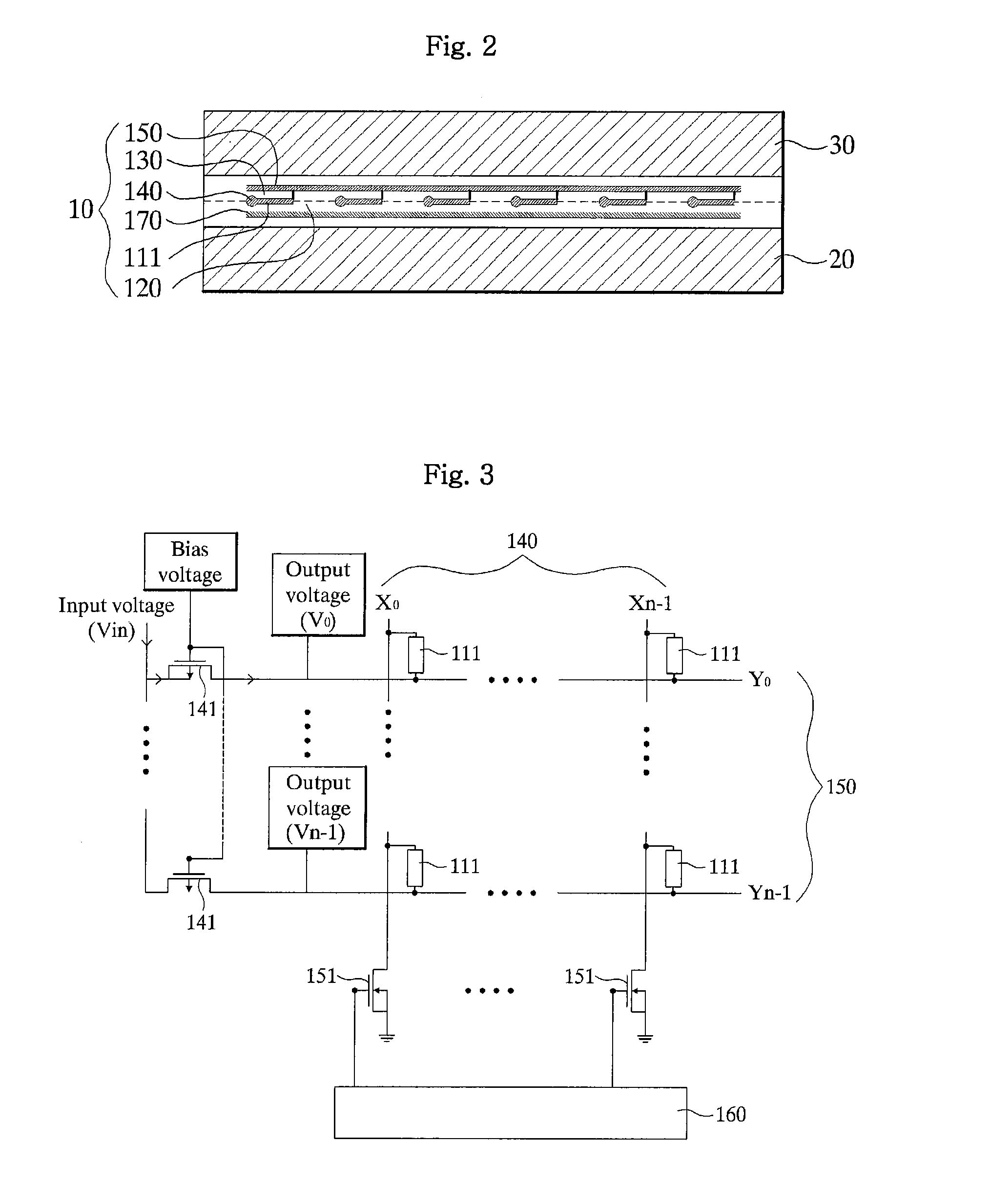
[0028]FIG. 1a is a perspective view showing a force or pressure sensor array using semiconductor strain gauges 100 according to an embodiment of the present invention, and FIG. 1b is an exploded perspective view showing the force or pressure sensor array in FIG. 1 decomposed into a layer structure. As shown in FIGS. 1a and 1b, the force or pressure sensor array according to an embodiment of the present invention comprises a substrate 10 and a pair of elastomer layers 20 and 30 bonded to both sides of the substrate. Here, a polymer film layer and semiconductor strain gauges 110 containing a plurality of elements 111 arranged in a specific array pattern are placed in the substrate 10, and a plurality of first and second signal lines respectively forming an electrode is provided in the substrate. In addition, the substrate 10 further includes a CMOS circuit layer 170 at the lower part of the substrate, where current sources 141 for flowing a constant current to the first signal l...


PUM

PropertyMeasurementUnit
thicknessaaaaaaaaaa
thicknessaaaaaaaaaa
thicknessaaaaaaaaaa

Abstract

The force or pressure sensor array of the present invention effectively has both flexibility and elasticity. Since the substrate itself is a kind of a polymer material, the substrate can be bent or expanded. Although silicon, which is a material of the semiconductor strain gauge, is easily broken and solid, mechanical flexibility can be secured if it is fabricated extremely thin. To this end, particularly, disclosed is a flexible force or pressure sensor array using semiconductor strain gauges 110, the sensor array comprising: a substrate 10 including: the semiconductor strain gauges 110 in which a plurality of elements formed in a certain array pattern is deformed by force or pressure, a pair of polymer film layers 120 and 130 having film surfaces contacted facing each other and containing the semiconductor strain gauge 110 between the film surfaces contacted with each other, and a pair of signal line layers formed on top and bottom surfaces of an insulating layer using either of the pair of polymer film layers 120 and 130 as the insulating layer and connected to the elements 111 of the array pattern to form electrodes, for fetching deformation signals outputted due to deformation of the elements 111 to outside; and a pair of elastomer layers 20 and 30 formed on both sides of the substrate 10 to contain the substrate 10 inside.

Description

TECHNICAL FIELD[0001]The present invention relates to a flexible force or pressure sensor array using a semiconductor strain gauge, and more specifically, to a force or pressure sensor array using a semiconductor strain gauge, a method of fabricating the force or pressure sensor array, and a method of measuring force or pressure using the force or pressure sensor array, in which a high-sensitive semiconductor strain gauge is used, and flexible and stabile polymer film layers and elastomer layers are configured.BACKGROUND ART[0002]In fabricating a force or pressure sensor array, conventionally, a strain gauge is configured using a Ni / Cr or Cu / Ni metal layer. However, this method is disadvantageous in that since a gauge factor is lower than that of a semiconductor strain gauge as much as 50 to 100 times, sensitivity is lowered as much.[0003]The semiconductor strain gauge is fabricated by injecting impurities into mono-crystalline or polycrystalline silicon, and since the gauge factor ...

Claims


Application Information

Patent Timeline
Patent Type & Authority Applications(United States)
IPC IPC(8): G01L1/22H01L21/00
CPCG01L1/2293
Inventor KIM, MIN SEOKPARK, YON-KYUKANG, DAE IMSONG, HAN WOOKLEE, SUNGJUNCHOI, IN-MOOK
Owner KOREA RES INST OF STANDARDS & SCI
Why Eureka
Try Eureka