Semiconductor device and method for manufacturing the same

a semiconductor and semiconductor technology, applied in the direction of semiconductor devices, semiconductor/solid-state device details, electrical equipment, etc., can solve the problems of reducing the efficiency of production of devices forming by low-precision design rules, reducing the efficiency of production, and restricting the integration of devices, etc., to achieve the effect of reducing warpage and reducing thickness

Active Publication Date: 2009-07-16
KK TOSHIBA
View PDF7 Cites 37 Cited by
  • Summary
  • Abstract
  • Description
  • Claims
  • Application Information

AI Technical Summary

Benefits of technology

[0012]The present invention has been made in view of these circumstances, and an object thereof is to provide a semiconductor device and a method for manufacturing the semiconductor device that can restrict warpage at the time of resin cure and can achieve a smaller thickness.

Problems solved by technology

However, there are restrictions on the devices that can be integrated.
For example, it is difficult to form a device containing a crystalline material such as GaAs on a Si substrate, because of the difference in lattice constant and the difference in linear expansion coefficient.
Also, a device such as a LSI requiring high-precision design rules and a device formed by low-precision design rules cannot be efficiently produced in the same procedures.
Therefore, the costs for development of a new device are high, and the development period is long.
Accordingly, the development cost is low, and the development period is short.
However, the problem with this technique is that the interposer and the chips are connected with bonding wires and bumps or the likes.
Therefore, it is difficult to achieve high density in chip arrangement, and to form minute wires and a thinner package.
Therefore, the device cannot be made thinner, and high integration cannot be achieved.
Therefore, the device cannot be made thinner, and higher integration cannot be achieved.

Method used


Image

  • Semiconductor device and method for manufacturing the same
  • Semiconductor device and method for manufacturing the same
  • Semiconductor device and method for manufacturing the same

Examples


first embodiment

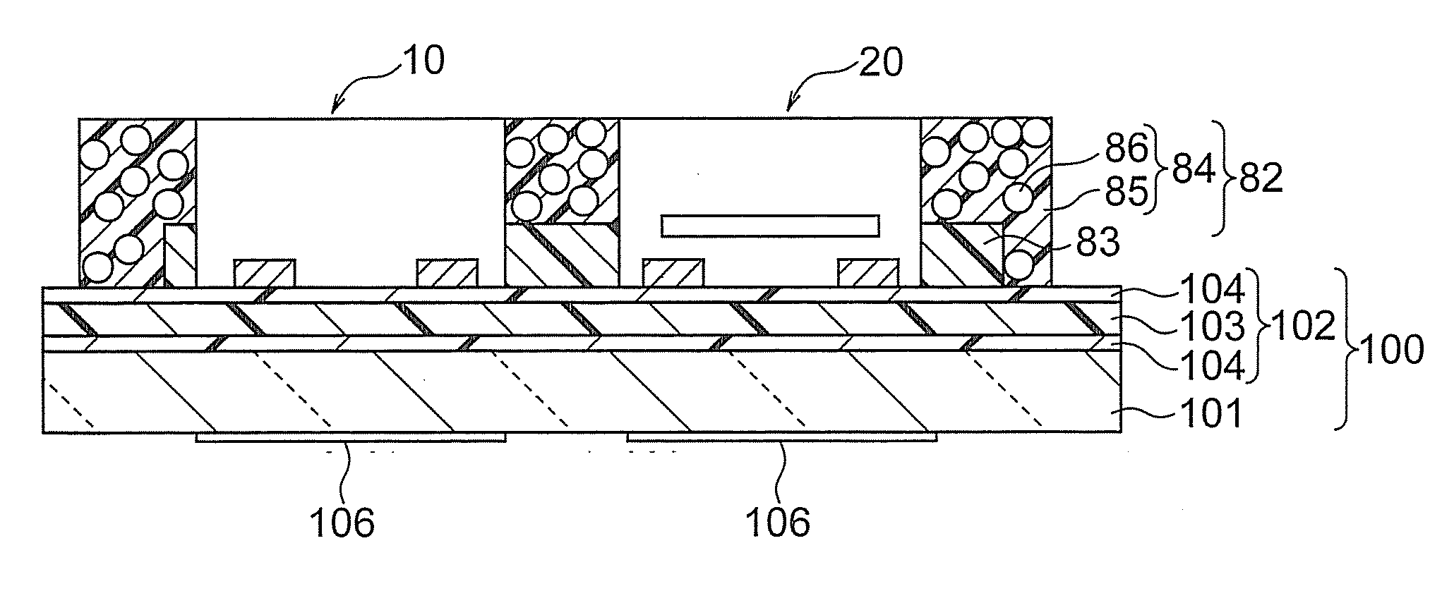
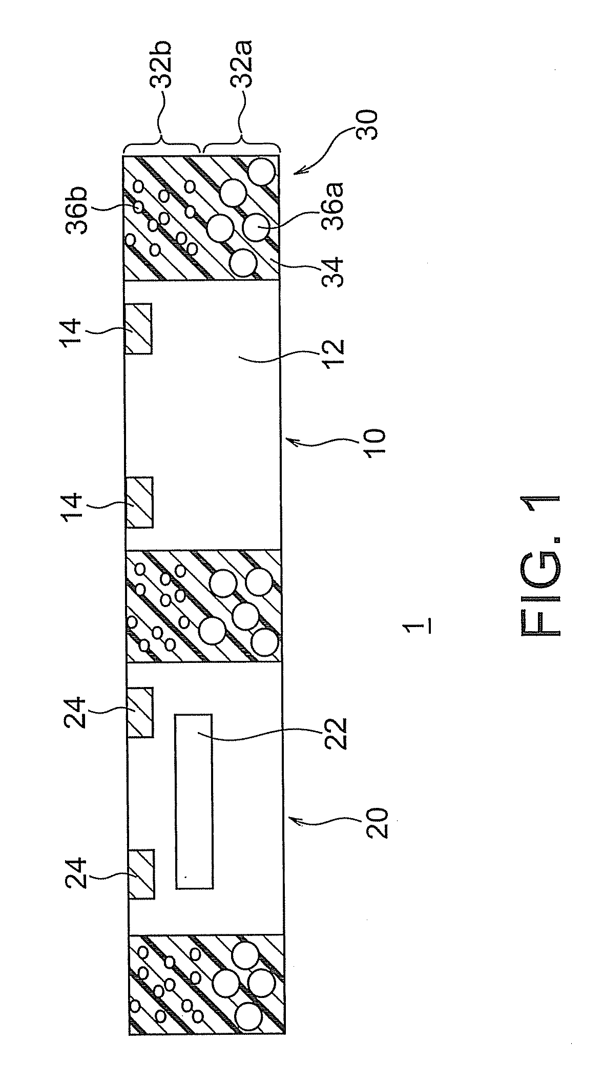
[0045]FIG. 1 illustrates a semiconductor device in accordance with a first embodiment of the present invention. The semiconductor device 1 of this embodiment includes a semiconductor chip 10, a MEMS chip 20, and adhesive layers 30 that are provided on the side faces of those chips and bond the semiconductor chip 10 and the MEMS chip 20. The semiconductor chip 10 contains a semiconductor device 12 (such as a CMOS device). Pads 14 that are electrically connected to the semiconductor device 12 are provided in the upper face of the semiconductor chip 10. The MEMS chip 20 contains a MEMS device 22. Pads 24 that are electrically connected to the MEMS device 22 are provided in the upper face of the MEMS chip 20. The adhesive layers 30 each have a stacked structure of adhesive films 32a and 32b that have different material constant modifiers contained in resin. The adhesive film 32a has a structure in which a filler 36a containing silica as the principal component with a relatively large me...

second embodiment

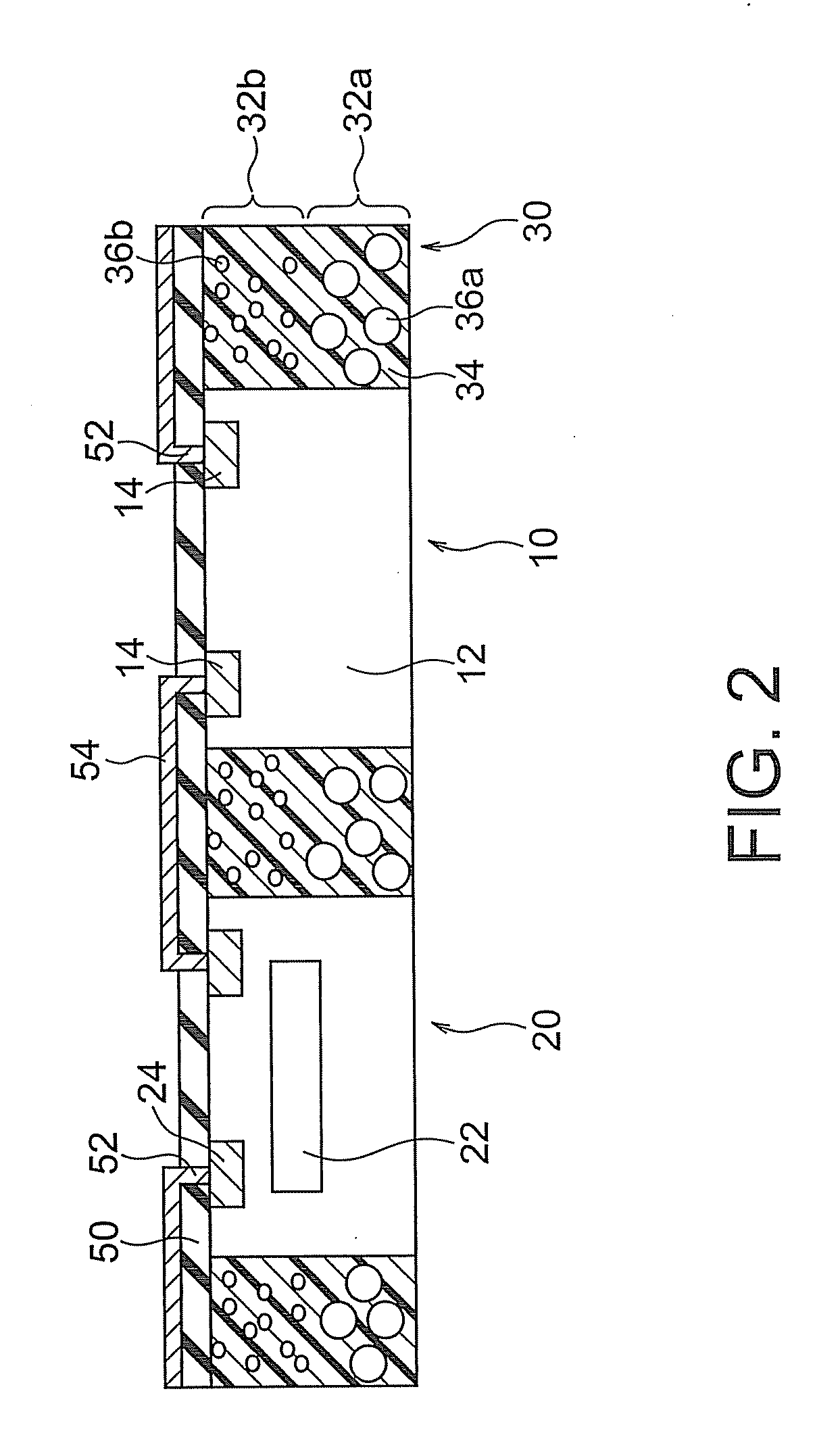
[0066]FIG. 12 illustrates a semiconductor device in accordance with a second embodiment of the present invention. The semiconductor device 1A of this embodiment is the same as the semiconductor device 1 of the first embodiment illustrated in FIG. 1, except that an adhesive film 32c is provided on the surfaces on the opposite side from the principal surfaces of the chips 10 and 20. The adhesive film 32c serves as a backing layer. The adhesive layer 30A that is provided between the semiconductor chip 10 and the MEMS chip 20, and bonds the semiconductor chip 10 and the MEMS chip 20 has a stacked structure formed with the adhesive film 32c, the adhesive film 32a, and the adhesive film 32b stacked in this order. The adhesive films 32a, 32b, and 32c contain at least two different material constant modifiers. The adhesive film 32b is a resin having a filler 36b added thereto. The filler 36b contains silica with a small mean particle size as the principal component. The adhesive film 32a is...

example 1

[0072]FIG. 1 shows a semiconductor device of Example 1 of the present invention. The semiconductor device 1 of this example includes a semiconductor chip 10, a MEMS chip 20, and an adhesive layer 30 that bonds the semiconductor chip 10 and the MEMS chip 20. The semiconductor chip 10 contains a semiconductor device 12 (such as a CMOS device). Pads 14 that are electrically connected to the semiconductor device 12 are provided in the upper face of the semiconductor chip 10. The MEMS chip 20 contains a MEMS device 22. Pads 24 that are electrically connected to the MEMS device 22 are provided in the upper face of the MEMS chip 20. The adhesive layer 30 has a stacked structure of adhesive films 32a and 32b that have different material constant modifiers contained in resin. The adhesive film 32a has a structure in which a filler 36a containing silica as the principal component with a relatively large mean particle size is added to the resin 34, and the adhesive film 32b has a structure in ...


PUM


Abstract

It is made possible to restrict warpage at the time of resin cure and achieve a smaller thickness. A semiconductor device includes: a first chip including a MEMS device and a first pad formed on an upper face of the MEMS device, the first pad being electrically connected to the MEMS device; a second chip including a semiconductor device and a second pad formed on an upper face of the semiconductor device, the second pad being electrically connected to the semiconductor device; and an adhesive portion having a stacked structure, and bonding a side face of the first chip and a side face of the second chip, the stacked structure including a first adhesive film formed by adding a first material constant modifier to a first resin, and a second adhesive film formed by adding a second material constant modifier to a second resin.

Description

CROSS-REFERENCE TO RELATED APPLICATION[0001]This application is based upon and claims the benefit of priority from prior Japanese Patent Application No. 2008-4100 filed on Jan. 11, 2008 in Japan, the entire contents of which are incorporated herein by reference.BACKGROUND OF THE INVENTION[0002]1. Field of the Invention[0003]The present invention relates to a semiconductor device and a method for manufacturing the semiconductor device.[0004]2. Related Art[0005]As digitalization and broadbandization have rapidly progressed in precision electronic devices such as portable telephone devices, portable information terminals, and digital appliances, there is an increasing demand for semiconductor devices with multiple functions, high-performance semiconductor devices, less expensive semiconductor devices, and high-density semiconductor devices. In this trend, there is a need for a novel mounting technique for mounting different kinds of devices such as logic devices, memories, sensors, and...

Claims


Application Information

Patent Timeline
Patent Type & Authority Applications(United States)
IPC IPC(8): H01L23/00H01L21/98
CPCB81C1/00238B81C1/00253H01L24/18H01L2924/19105H01L2224/24195H01L2924/18162H01L2924/1461H01L24/96H01L2224/24137H01L2924/10253H01L2924/00H01L21/568H01L2224/04105H01L2924/15788H01L2924/3511H01L23/295H01L24/19H01L23/3135
Inventor IIDA, ATSUKOONOZUKA, YUTAKAITAYA, KAZUHIKO
Owner KK TOSHIBA
Why Eureka
Try Eureka