Warpage control structure for metal base plate, semiconductor module, and inverter device

a control structure and metal base plate technology, applied in semiconductor devices, semiconductor/solid-state device details, electrical apparatus, etc., can solve the problems of warpage occurring in the metal base plate after joining and difficulty in warping treatmen

Pending Publication Date: 2022-05-19
MITSUBISHI ELECTRIC CORP
View PDF0 Cites 0 Cited by
  • Summary
  • Abstract
  • Description
  • Claims
  • Application Information

AI Technical Summary

Benefits of technology

[0015]According to the present invention, when the metal base plate is subjected to temperature change from room temperature to high temperature, due to the difference of the linear expansion coefficients between the metal base plate and the dissimilar metal layer, the metal base plate expands with respect to the dissimilar metal layer, and the metal base plate warps in the direction projecting toward the side opposite to the surface thereof to which the insulation substrate is joined. When the metal base plate and the insulation substrate are subjected to temperature change from high temperature to room temperature after the insulation substrate is jointed to the surface of the dissimilar metal layer with the joining material in this state, due to the difference of the linear expansion coefficients between the insulation substrate and the metal base plate, the metal base plate contracts with respect to the insulation substrate, and the metal base plate warps in the direction projecting toward the side of the surface thereof to which the insulation substrate is joined.
[0016]In the temperature change from room temperature to high temperature and the temperature change from high temperature to room temperature, the metal base plate warps in directions opposite to each other, and thus the warpage in each of the directions is cancelled out. In this manner, the warpage of the metal base plate occurring in the temperature change from high temperature to room temperature can be controlled.
[0017]These and other objects, features, aspects and advantages of the present invention will become more apparent from the following detailed description of the present invention when taken in conjunction with the accompanying drawings.

Problems solved by technology

However, when the insulation substrate is joined to the metal base plate using solder, warpage occurs in the metal base plate after joining.
Warping treatment of causing initial warping in the metal base plate is generally performed in order to cause the warpage of the metal base plate to project toward the side of the non-joining surface; however, when there is a fin or the like in the non-joining surface of the metal base plate, performing the warping treatment is difficult.

Method used


Image

  • Warpage control structure for metal base plate, semiconductor module, and inverter device
  • Warpage control structure for metal base plate, semiconductor module, and inverter device
  • Warpage control structure for metal base plate, semiconductor module, and inverter device

Examples


embodiment

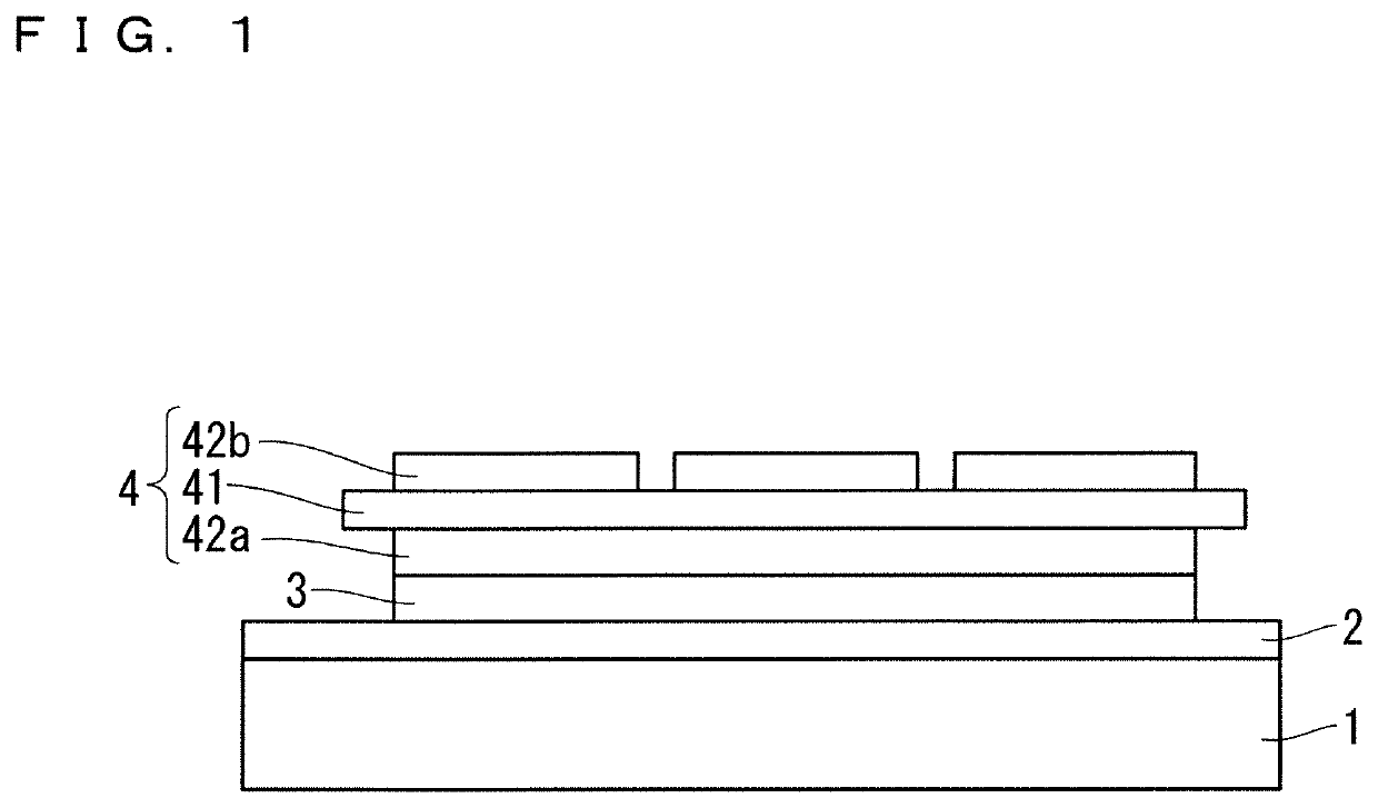
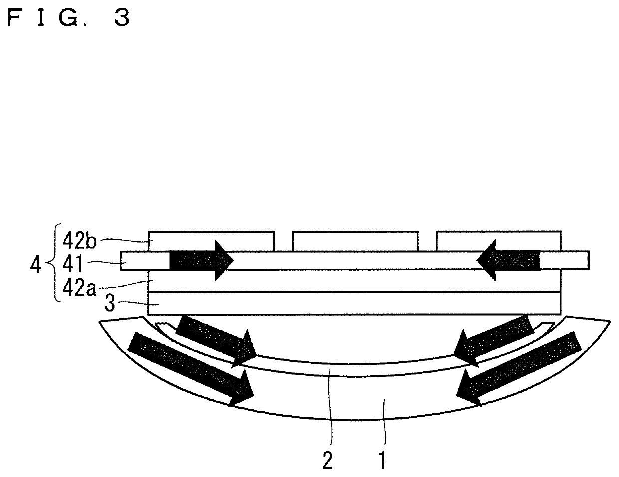
[0024]An embodiment of the present invention will be described below with reference to the drawings. FIG. 1 is a side view of a warpage control structure for a metal base plate according to an embodiment.

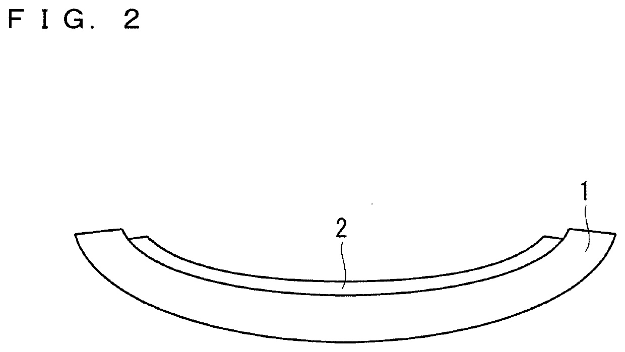
[0025]As illustrated in FIG. 1, the warpage control structure for the metal base plate constitutes a part of a semiconductor module, and includes a metal base plate 1, a dissimilar metal layer 2, and an insulation substrate 4.

[0026]The metal base plate 1 has a square shape of approximately 100 mm×100 mm in plan view, and has a thickness of from 3.5 mmt to 4.0 mmt. Further, as a material of the metal base plate 1, a highly thermally conductive material such as aluminum, aluminum alloy, or copper is desirable. In the present embodiment, aluminum is selected in order to reduce total weight.

[0027]The dissimilar metal layer 2 is formed on the entire surface of the metal base plate 1, or only in the region of the surface of the metal base plate 1 where the insulation substrate 4 is joined...


PUM

PropertyMeasurementUnit
thicknessaaaaaaaaaa
temperatureaaaaaaaaaa

Abstract

The object is to provide a technology of controlling warpage of a metal base plate occurring in temperature change from high temperature to room temperature by causing warpage in the metal base plate in temperature change from room temperature to high temperature. A dissimilar metal layer is formed on a surface of a metal base plate. An insulation substrate is joined to a surface of the dissimilar metal layer with a joining material being provided between the insulation substrate and the surface of the dissimilar metal layer, and includes metal plates disposed on both surfaces. α1>α3>α2 is satisfied, where α1 represents a linear expansion coefficient of the metal base plate, α2 represents a linear expansion coefficient of the dissimilar metal layer, and α3 represents a linear expansion coefficient of the metal plates.

Description

TECHNICAL FIELD[0001]The present invention relates to a technology of controlling warpage occurring when an insulation substrate is joined to a metal base plate in a high temperature state.BACKGROUND ART[0002]In a semiconductor module, a structure and a method of joining an insulation substrate to a metal base plate has been adopted. As a general joining method, inexpensive solder joining is in many cases used. However, when the insulation substrate is joined to the metal base plate using solder, warpage occurs in the metal base plate after joining. This is because of the following reason: In temperature change from room temperature to high temperature when solder is melted, warpage does not occur in the metal base plate, whereas in temperature change from high temperature to room temperature when the solder solidifies, significant warpage occurs in the metal base plate due to a difference of linear expansion coefficients between the metal base plate and the insulation substrate. In...

Claims


Application Information

Patent Timeline
Patent Type & Authority Applications(United States)
IPC IPC(8): H01L23/00H01L25/065
CPCH01L24/32H01L23/562H01L2224/32245H01L2924/3511H01L25/0657H01L23/14H01L23/3735H01L21/4875
Inventor KAWASE, TATSUYAHAYASHI, KEIWADA, FUMIOMAEDA, ATSUSHI
Owner MITSUBISHI ELECTRIC CORP
Why Eureka
Try Eureka