Method for manufacturing thin film compound solar cell

a solar cell and compound technology, applied in the field of manufacturing a thin film compound solar cell, can solve the problems of corroding metallic ribbons, hydrofluoric acid, separation of rear surface electrodes from compound semiconductor layers, etc., and achieve the effect of improving the adhesive property of each electrode and reducing contact resistan

Inactive Publication Date: 2014-02-20
SHARP KK
View PDF6 Cites 1 Cited by
  • Summary
  • Abstract
  • Description
  • Claims
  • Application Information

AI Technical Summary

Benefits of technology

[0030]According to the present invention, since the surface electrode and the rear surface electrode are annealed, it is possible to improve the adhesive property of each of the electrodes and to reduce the contact resistance of each of the electrodes. Further, the heat-resistant base material is used. Thus, after the reinforcing material is removed, the electrode can be annealed in the state where the base material is attached. As a result, the reinforcing material is not heat-treated, and hence the reinforcing material can be reused.
[0031]Further, a highly heat-resistant film, such as polyimide, is used as the base material, and hence the film itself serves as the supporting body. Therefore, even when an external force is applied, the photovoltaic cell is not broken. Further, since the amount of warpage of the photovoltaic cell is changed according to the film thickness, it is possible to control the warpage of the cell during the film forming process.

Problems solved by technology

Therefore, there is a problem that the rear surface electrode is separated from the compound semiconductor layer.
Thus, there is a problem that, when the resin is exposed to the organic solvent and water, the exposed resin penetrates into the interface between the surface film and the resin, or into the interface between the compound semiconductor layer and the resin, so as to make the surface film liable to be separated from the compound semiconductor layer.
However, hydrofluoric acid reacts with the metallic ribbon to corrode the metallic ribbon.
This results in a problem that the number of processes is increased.
However, in the above-described compound solar cell described in Patent Document, the surface film as the base material is not provided, and hence the problem of separation of the surface film does not occur.

Method used


Image

  • Method for manufacturing thin film compound solar cell
  • Method for manufacturing thin film compound solar cell
  • Method for manufacturing thin film compound solar cell

Examples


Embodiment Construction

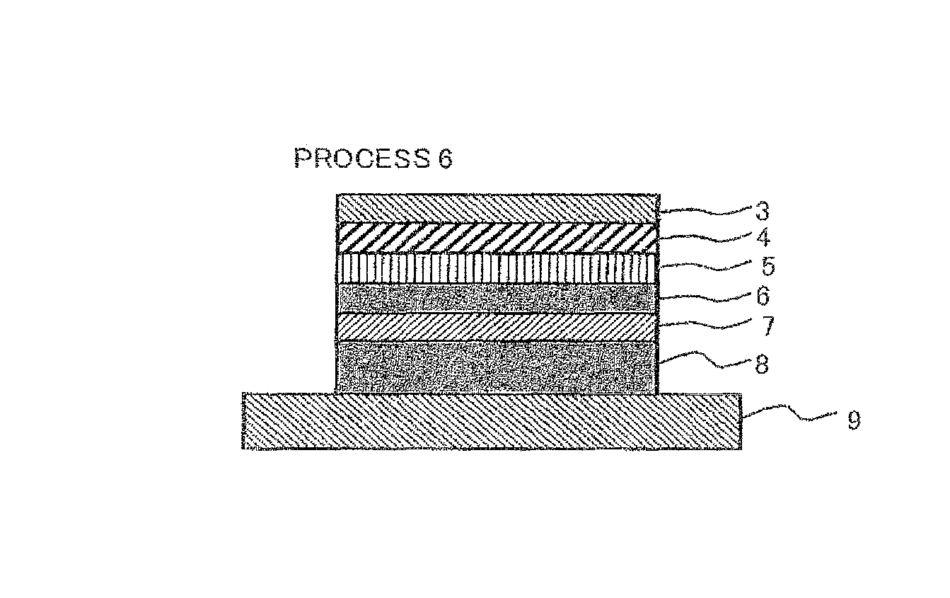
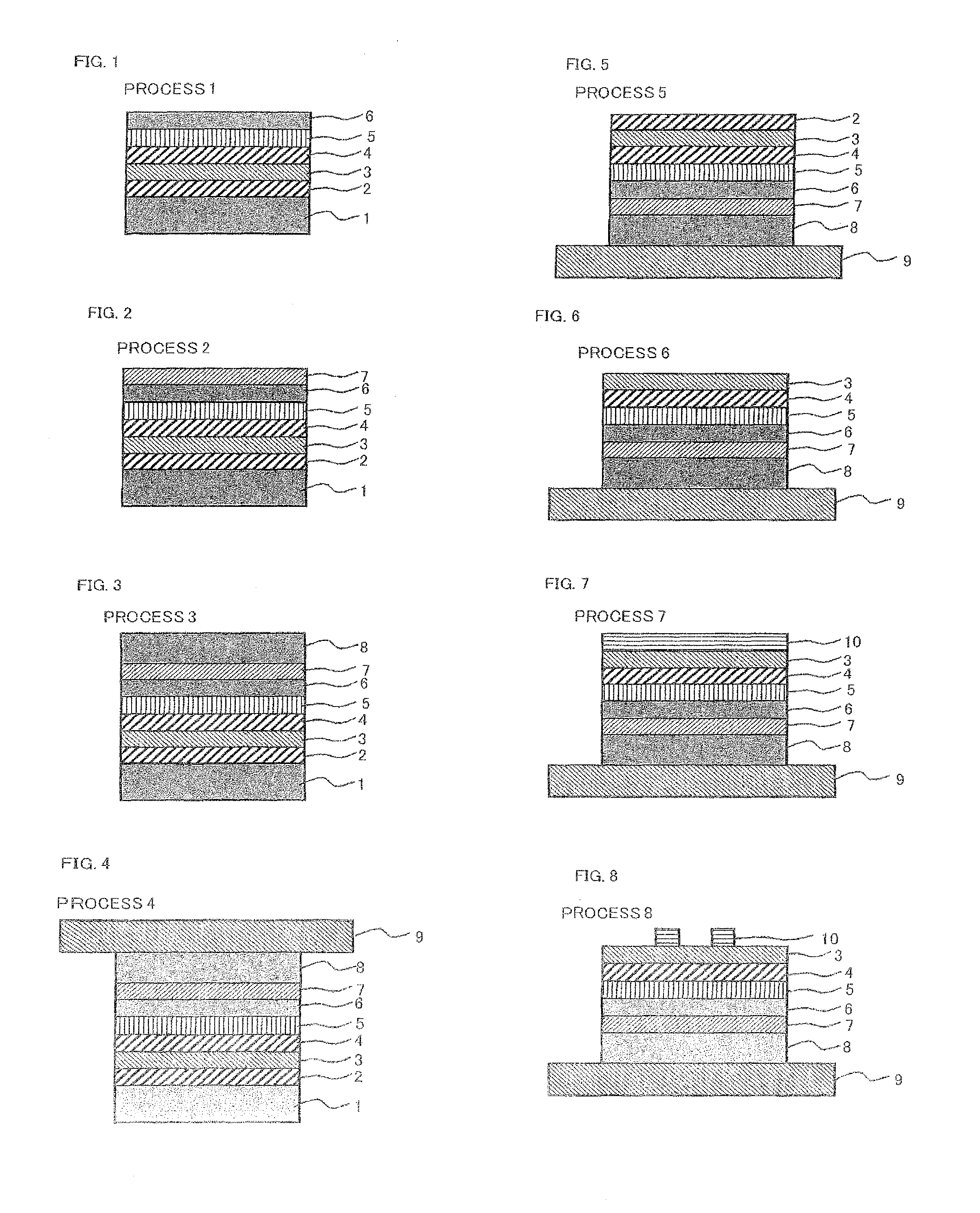
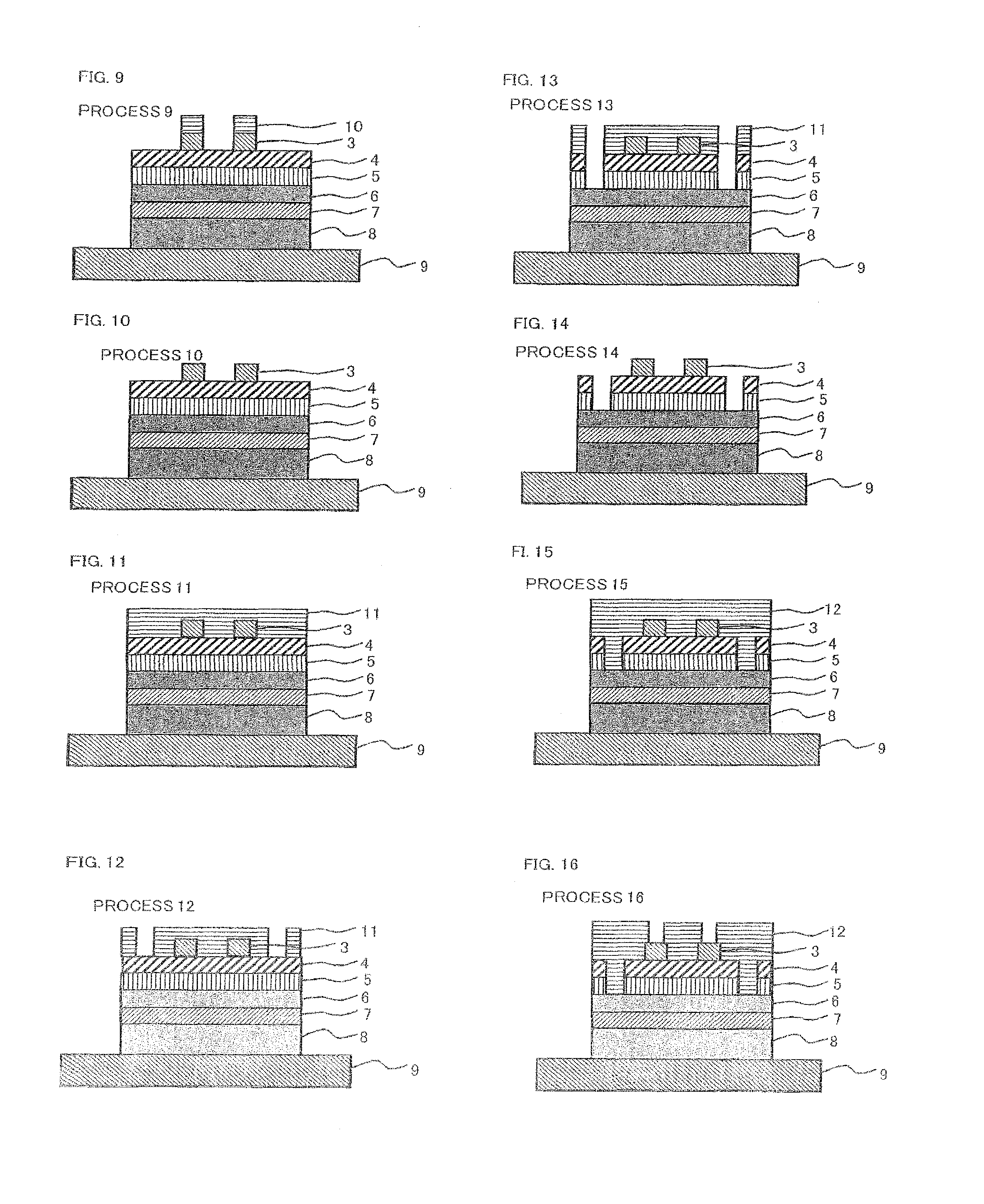
[0077]A thin film compound solar cell according to the present embodiment has a structure including: a cell main body in which at least one PN junction is formed by laminating a plurality of compound semiconductor layers, each having a different chemical composition; a surface electrode which is formed on the light receiving surface of the cell main body; a rear surface electrode which is formed on the opposite surface of the cell main body; and a base material for the thin film solar cell. The base material is formed on the opposite surface of the cell main body, and the rear surface electrode is sandwiched between the cell main body and the base material.

[0078]A method for manufacturing the solar cell having this structure will be described. In process 1 shown in FIG. 1, a compound semiconductor layer made of single crystal thin films is formed by laminating, on a substrate 1, an etching-stop layer 2 for suppressing infiltration of an etching solution from the side of the substrat...


PUM

PropertyMeasurementUnit
thicknessaaaaaaaaaa
temperatureaaaaaaaaaa

Abstract

To manufacture a thin film compound solar cell which can improve the adhesive property of electrodes even when being provided with a base material, and which prevents the base material from being separated. A cell main body configured by laminating a plurality of compound semiconductor layers is formed on a substrate. A rear surface electrode 7 is formed on the cell main body, and a rear surface film 8 as the base material is formed on the rear surface electrode 7. A reinforcing material 9 is attached on the rear surface film 8. The substrate is separated from the cell main body, and the cell main body is mesa-etched. A surface electrode 13 is formed on a contact layer 3 after the etching. The reinforcing material 9 is separated, and the surface electrode 13 is annealed. The formed thin film compound solar cell is separated into a plurality of solar cell elements.

Description

CROSS REFERENCE TO RELATED APPLICATIONS[0001]This application is a divisional of U.S. application Ser. No. 13 / 202,678, filed Aug. 22, 2011, which is the U.S. national phase of International Application No. PCT / JP2010 / 052655, filed Feb. 22, 2010, which designated the U.S. and claims priority to Japanese Application No. 2009-044415, filed Feb. 26, 2009, the entire contents of each of which are hereby incorporated by reference.TECHNICAL FIELD[0002]The present invention relates to a method for manufacturing a thin film compound solar cell having a cell main body in which at least one PN junction is formed by a plurality of compound semiconductor layers, each having a different chemical composition.BACKGROUND ART[0003]A conventional thin film compound solar cell is configured such that a surface electrode is provided on a light receiving surface of a cell main body formed by laminating a plurality of compound semiconductor layers, and such that a rear surface electrode is provided on the...

Claims


Application Information

Patent Timeline
Patent Type & Authority Applications(United States)
IPC IPC(8): H01L31/18
CPCH01L31/18H01L31/0392H01L31/0693Y02E10/544H01L31/022425H01L31/03926H01L31/1864H01L31/06875H01L31/1892Y02P70/50
Inventor KODAMA, TOMOYA
Owner SHARP KK
Why Eureka
Try Eureka