Method of manufacturing a semiconductor light emitting device utilizing a nitride III-V compound semiconductor substrate

a technology of compound semiconductor substrate and semiconductor light emitting device, which is applied in the direction of semiconductor lasers, crystal growth process, polycrystalline material growth, etc., can solve the problems adverse effect of large warpage of sapphire substrate, and uneven distance between photo mask and resist, etc., to achieve limit the warpage effect of substra

Inactive Publication Date: 2006-04-11
SONY CORP
View PDF6 Cites 1 Cited by
  • Summary
  • Abstract
  • Description
  • Claims
  • Application Information

AI Technical Summary

Benefits of technology

[0013]It is therefore an object of the invention to provide a nitride III-V compound semiconductor substrate and its manufacturing method capable of limiting warpage of substrates not to exceed 70 μm.
[0014]A further object of the invention is to provide a method of manufacturing a semiconductor light emitting device that can be used when manufacturing the semiconductor light emitting device by using a nitride III-V compound semiconductor substrate made by forming a nitride III-V compound semiconductor layer on a substrate of a material different from the nitride III-V compound semiconductor layer, and can limit warpage of the substrate not to exceed 70 μ, thereby to successfully carry out exposure in the lithographic process and polishing of the bottom surface of the substrate.
[0015]A still further object of the invention is to provide a method of manufacturing a semiconductor device that can be used when manufacturing the semiconductor device by using a nitride III-V compound semiconductor substrate made by forming a nitride III-V compound semiconductor layer on a substrate of a material different from the nitride III-V compound semiconductor layer, and can limit warpage of the substrate not to exceed 70 μm, thereby to successfully carry out exposure in the lithographic process and polishing of the bottom surface of the substrate.
[0021]Also from the viewpoint of improving evenness of the temperature distribution along the substrate plane during crystal growth, warpage of the substrate must be minimized. Evenness of the temperature distribution is required for ensuring evenness of the Al composition distribution of the cladding layer of the GaN compound semiconductor laser, distribution of the thickness of each layer and distribution of composition of the active layer (corresponding to the distribution of the emission wavelength). Especially, the active layer needs accurate temperature control and temperature distribution control because the emission wavelength changes by approximately 1 nm with change of the growth temperature by 1° C. If warpage occurs in the substrate, the temperature distribution on the substrate surface increases, and the composition distribution of the active layer (distribution of the emission wavelength) also increases. This results in increasing the region where the emission wavelength deviates from the desired wavelength and decreasing the production yield. If Z is decreased to 0.011 or less and the warpage is limited not to exceed 70 μm, then the production yield can be enhanced also from the above-mentioned viewpoint.

Problems solved by technology

This large warpage of the sapphire substrate adversely works against exposure in a manufacturing process of a GaN compound semiconductor laser and polishing of the bottom surface of the sapphire substrate.
If the sapphire substrate largely warps as mentioned above, distance between the photo mask and the resist may become uneven within the area of the substrate, or a dimensional deviation may be produced between the photo mask and the substrate within the area of the substrate.
Thus the mask cannot accurately fit the entire surface of the substrate.
As a result, especially when a base GaN layer is laterally grown on the sapphire substrate by ELO (epitaxial lateral overgrowth) and GaN compound semiconductor layers forming a laser structure are grown thereon by crystal growth, it is difficult to form a ridge in a less-defective region (wing portion) between a seed crystal and a coalescing portion of the lateral growth, and the ridge often deviates from the wing portion.
Therefore, this problem adversely affects the laser properties, and in particular, its lifetime, and also degrades the production yield.
However, if the sapphire substrate largely warps as mentioned above, it often cracks during polishing.
Furthermore, if the warpage of the sapphire substrate is large during crystal growth of the GaN compound semiconductor layers, because of uneven temperature distribution along the plane, the resulting GaN compound semiconductor layers become uneven in composition and thickness.

Method used


Image

  • Method of manufacturing a semiconductor light emitting device utilizing a nitride III-V compound semiconductor substrate
  • Method of manufacturing a semiconductor light emitting device utilizing a nitride III-V compound semiconductor substrate
  • Method of manufacturing a semiconductor light emitting device utilizing a nitride III-V compound semiconductor substrate

Examples


first embodiment

[0071]Next explained is a manufacturing method of the GaN compound semiconductor laser according to the invention.

[0072]This embodiment uses a c-plane sapphire substrate 1 having a thickness x in the range from 600 to 1000 μm, e.g. 640 μm, and the diameter of 50 mm, and satisfies 0

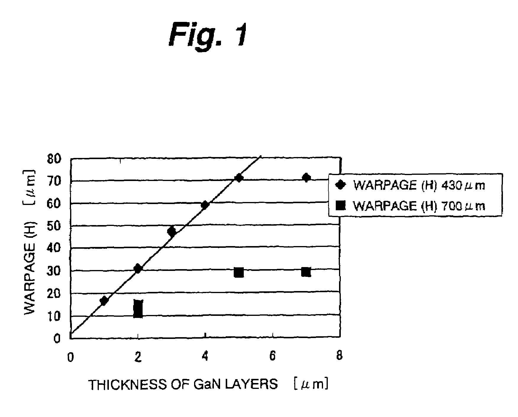
[0073]More specifically, preparing the c-plane sapphire substrate 1 whose surface is cleaned by thermal cleaning beforehand, the undoped GaN buffer layer 2 is grown on the c-plane sapphire substrate 1 by MOCVD under a temperature around 500° C., for example. After that, the undoped GaN layer 3 is grown under the growth temperature 1000° C., for example, by a lateral growth technique such as ELO.

[0074]Subsequently, using MOCVD, the n-type GaN contact layer 4, n-type AlGaN cladding layer 5, n-type GaN waveguide layer 6, active layer 7 having the undoped Ga1−xInxN / Ga1−yInyN multiquantum well structure, undoped In...

second embodiment

[0092]Next explained is a manufacturing method of a GaN compound semiconductor laser according to the invention.

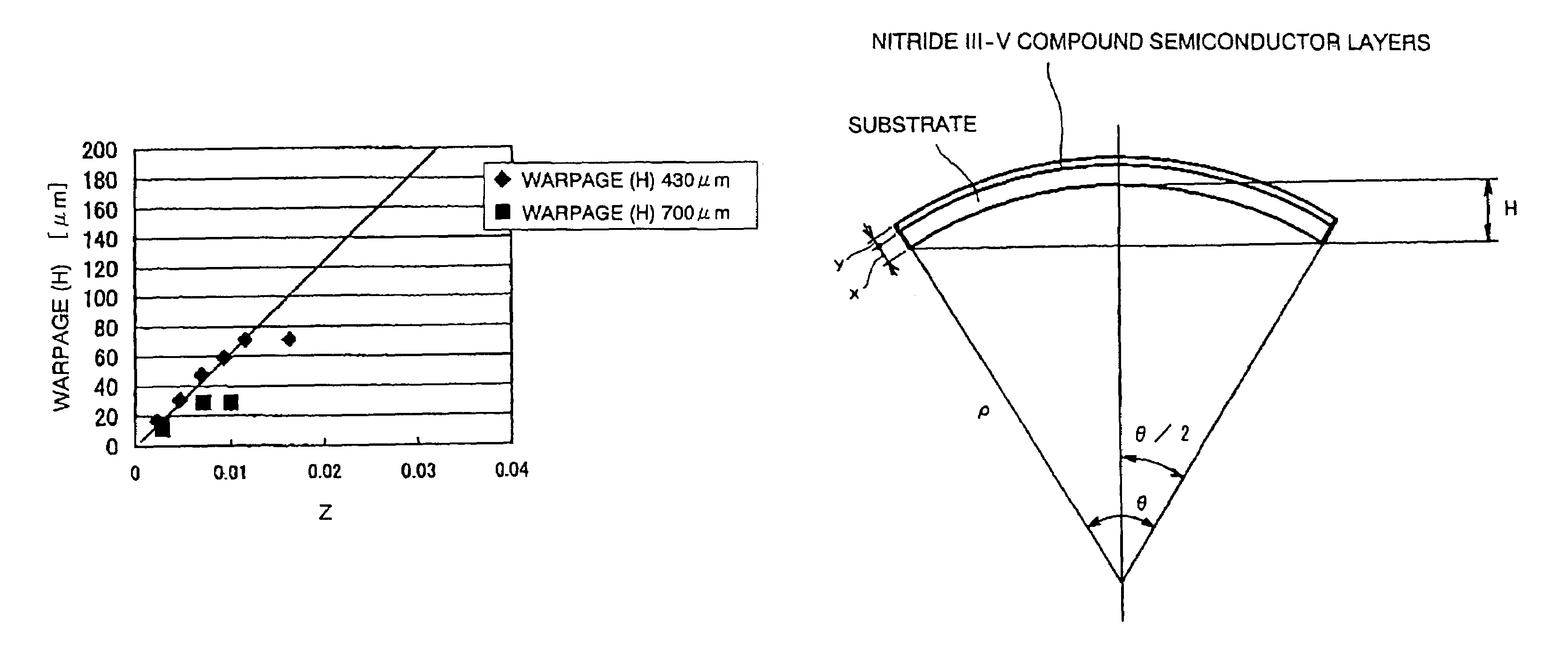
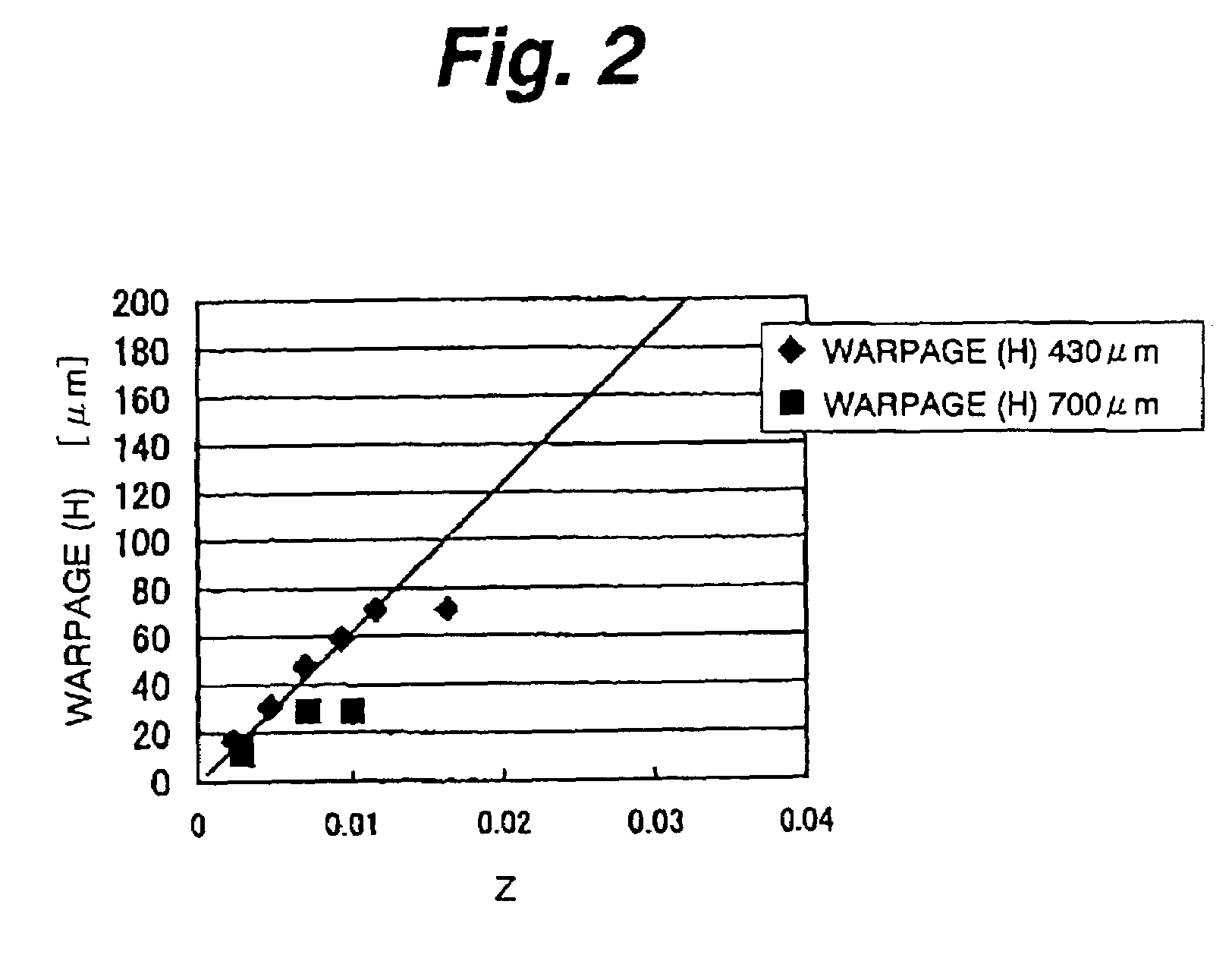
[0093]The second embodiment uses a c-plane sapphire substrate 1 having the thickness of 430 μm and having a diameter D satisfying the equation

0DCZ)cos−1(1−HCZ)

and grows GaN compound semiconductor layers, 6.4 μm thick in total, on the c-plane sapphire substrate 1 similarly to the first embodiment. If that equation is substituted by C=0.20567 cm−1, H=70 μm=70×10−4 cm, Z=6.4 / 430=0.0149, it results in

0

[0094]Assume here that D satisfying the inequality is 4 cm. That is, in the second embodiment, a c-plane sapphire substrate 1 having the diameter of 4 cm and the thickness of 430 μm is used to manufacture the GaN compound semiconductor laser.

[0095]The other features of the second embodiment are common to those of the first embodiment, and are omitted from explanation.

[0096]The second embodiment also ensures the same advantages as those of the first embodiment.

[0097]Here...


PUM

PropertyMeasurementUnit
thicknessaaaaaaaaaa
thicknessaaaaaaaaaa
thicknessaaaaaaaaaa

Abstract

When GaN or other nitride III-V compound semiconductor layers are grown on a substrate such as a sapphire substrate, thickness x of the substrate relative to thickness y of the nitride III-V compound semiconductor layers is controlled to satisfy 0<y / x≦0.011 and x≧450 μm. Alternatively, if the maximum dimension of the substrate is D (cm), its warpage H is in the range of 0<H≦70×10−4 (cm), and Z=y / x, D is controlled to satisfy the relation 0<D<(2 / CZ)cos−1(1−HCZ), where C (cm−1) is the proportionality constant when the radius of curvature of the substrate ρ (cm) is expressed as 1 / ρ=CZ.

Description

[0001]The present application is a divisional of the patent application Ser. No. 10 / 288,181, filed on Aug. 27, 2002, now U.S. Pat. No. 6,829,270.BACKGROUND OF THE INVENTION[0002]1. Field of the Invention[0003]This invention relates to a nitride III-V compound semiconductor substrate, its manufacturing method, a method of manufacturing a semiconductor light emitting device and a method of manufacturing a semiconductor device, which are especially suitable for use in manufacturing semiconductor lasers and light emitting diodes, or electron transporting devices.[0004]2. Description of the Related Art[0005]In recent years, semiconductor lasers using nitride III-V compound semiconductors such as AlGaInN (hereinbelow called GaN compound semiconductor lasers) have been under active research and developments in the hope of making semiconductor lasers capable of emitting light over the range from the blue region to the ultraviolet region necessary for enhancing the density of optical discs. ...

Claims


Application Information

Patent Timeline
Patent Type & Authority Patents(United States)
IPC IPC(8): H01L21/00H01L29/22C30B29/38C30B25/02C30B25/18C30B29/40H01L21/20H01L33/00H01L33/06H01L33/32H01S5/323H01S5/343
CPCC30B25/02C30B25/18C30B29/40H01L33/007H01L21/02458H01L21/0254H01L21/02647H01L21/0242
Inventor SUZUKI, YASUHIKOASANO, TAKEHARUTAKEYA, MOTONOBUGOTO, OSAMUIKEDA, SHINROSHIBUYA, KATSUYOSHI
Owner SONY CORP
Why Eureka
Try Eureka