Alignment verification for c4np solder transfer

a technology of alignment verification and solder transfer, which is applied in the direction of printed circuits, electrical equipment, semiconductor devices, etc., can solve the problems of misalignment of more than 30 m in any direction, distortion of this ideal, and realizing the loss of yield

Inactive Publication Date: 2009-07-16
IBM CORP
View PDF5 Cites 6 Cited by
  • Summary
  • Abstract
  • Description
  • Claims
  • Application Information

AI Technical Summary

Benefits of technology

[0020]providing an electronic substrate containing pads in an array to which pads the solder in the mold is to be transferred, the mold array corresponding to the substrate pad array and the substrate having an inactive area having one or more inactive pads;
[0021]depositing a material around the periphery of the one or more inactive pads, which material reacts with molten solder;

Problems solved by technology

If these are misaligned, then bridges between C4's or missing C4's are seen and a yield loss is realized.
However, during the ramping up of the temperature and the motion that occurs when moving a wafer and mold into contact as well as aberrations in the optic system, some distortion from this ideal is seen.
If a wafer has a 150 micron pitch between capture pads, a misalignment of more than about 30 μm in any direction, can be disastrous.
There are no solutions to this problem to the best of our knowledge.

Method used


Image

  • Alignment verification for c4np solder transfer
  • Alignment verification for c4np solder transfer
  • Alignment verification for c4np solder transfer

Examples


Embodiment Construction

)

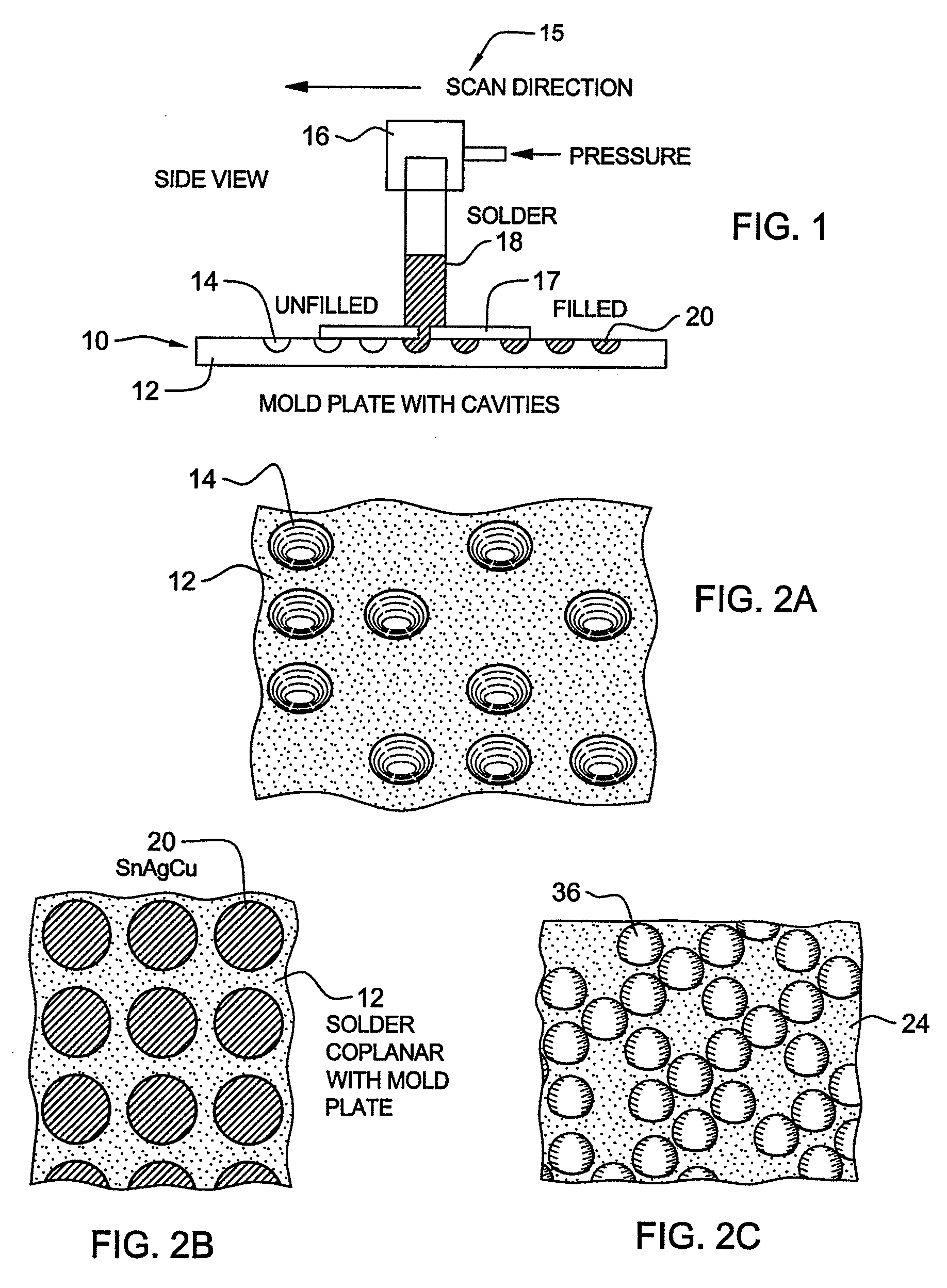
[0052]In describing the preferred embodiment of the present invention, reference will be made herein to FIGS. 1-8 of the drawings in which like numerals refer to like features of the invention.

[0053]Various solders may be readily processed using the method of the invention and these include lead and lead-free binary, ternary and quaternary alloys. Lead-free alloys are of particular commercial significance and for convenience the following description will be directed to such lead-free alloys although it will be appreciated by those skilled in the art that any suitable solder may be readily processed using the method of the invention. Exemplary lead-free alloys include Sn-1.8% Ag, Sn-0.5% Ag and Sn-0.7% Cu. Also, in particular, the following description will be directed to tin containing lead-free alloys since these are likewise of significant commercial interest and an efficient method of providing solder interconnects with these alloys is of important commercial consideration.

[005...


PUM

PropertyMeasurementUnit
diameteraaaaaaaaaa
diameteraaaaaaaaaa
diameteraaaaaaaaaa

Abstract

A method is provided for the making of interconnect solder bumps on a wafer or other electronic device. The method is particularly useful for the well-known C4NP interconnect technology and determines if any off-set resulted between the solder mold array and the wafer capture array during the transfer process. The amount of off-set enables the operator to adjust the transfer tool before solder transfer to compensate for the off-set caused by the transfer process and provides a more cost-effective and efficient solder transfer process. A solder reactive material surrounding the capture pads is used to determine where the solder reacts with the solder reactive material showing the off-set resulting from the transfer process. Copper is a preferred solder reactive material.

Description

BACKGROUND OF THE INVENTION[0001]1. Field of the Invention[0002]The present invention relates to the making of interconnect solder bumps on a wafer or other electronic device, and, in particular, to verifying the alignment between a solder containing mold and the capture pads on a transfer wafer after the transfer of the solder in the mold to the capture pads using the C4NP interconnect technology.[0003]2. Description of Related Art[0004]Forming an electronic package assembly whereby an electrical component such as an integrated circuit chip is electrically and mechanically connected to a substrate, a card, or board, another chip or another electronic part is well known in the art. This technology is generally termed surface mount technology (SMT) and has gained acceptance as the preferred means of making electronic package assemblies. The interconnect technology is commonly known as ball grid array packaging, C4 flip chip interconnect, multi-chip modules, multilayer and micro via p...

Claims


Application Information

Patent Timeline
Patent Type & Authority Applications(United States)
IPC IPC(8): H01L21/441
CPCH01L24/11H01L2224/11334H01L2224/16H01L2924/01004H01L2924/01013H01L2924/01027H01L2924/01029H01L2924/01033H01L2924/01047H01L2924/01078H01L2924/01079H01L2924/01082H01L2924/14H05K3/3457H05K2203/0113H05K2203/0338H01L2924/01006H01L2924/014H01L2924/00013H01L2224/13099H01L2224/29099H01L2224/05022H01L2224/05001H01L2224/05572H01L2224/051H01L2924/00014H01L24/06H01L24/05H01L24/13H01L2224/05599
Inventor GORRELL, JERRY A.KNICKERBOCKER, SARAH H.REDDY, SRINIVASA S.N.
Owner IBM CORP
Why Eureka
Try Eureka