Manufacturing method for a display device

a display device and manufacturing method technology, applied in non-linear optics, instruments, other domestic objects, etc., can solve the problems of display surface darkening, and inability to perform backlight maintenan

Inactive Publication Date: 2009-07-23
SEIKO INSTR INC
View PDF2 Cites 102 Cited by
  • Summary
  • Abstract
  • Description
  • Claims
  • Application Information

AI Technical Summary

Benefits of technology

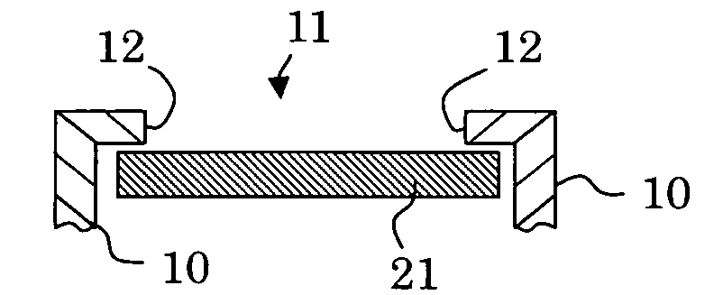
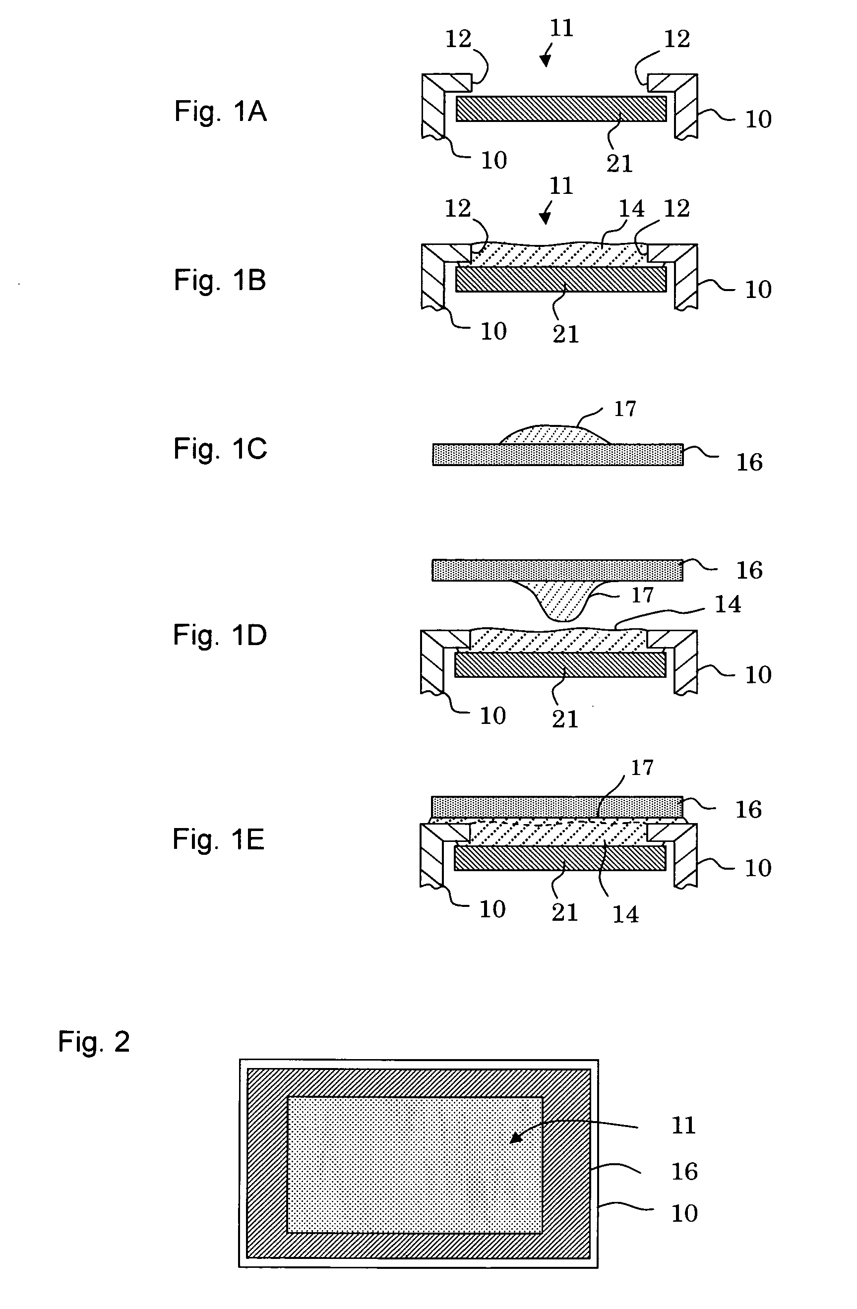
[0010]In order to solve the above-mentioned problems, in the present invention, a display panel is disposed inside a frame body having an opening on its top portion in adjacent to an end portion of the opening of the frame body, and then a first adhesive layer is formed by filling a first adhesive on an exposed surface of the display panel, which is exposed from the opening of the frame body. A step between the opening end portion of the frame body and a surface of the display panel is filled by the first adhesive layer, whereby a void can be prevented from being generated in an upper end corner portion

Problems solved by technology

However, when an air layer is interposed between the display panel and the cover glass or the touch panel, light is reflected on the surface of the display panel or on a bottom surface of the cover glass or the touch panel, which causes a problem in that the display surface is darkened due to reflection loss.
In the case where there is the gap between the upper end portion 66 of the frame body 60 and the upper polarizing plate 55 or the upper glass substrate 51, as indicated by an arrow 63, the tra

Method used


Image

  • Manufacturing method for a display device
  • Manufacturing method for a display device
  • Manufacturing method for a display device

Examples


embodiment 1

[0042]The manufacturing method for a display device according to this embodiment is described with reference to FIGS. 4A to 4E. FIG. 4A illustrates a cross-sectional structure of a liquid crystal panel 8 and the frame body 10, which illustrates a disposing step. In the liquid crystal panel 8, an upper substrate 1 made of glass is bonded to a lower substrate 2 made of glass to opposed to each other through a sealing material 4, and a liquid crystal layer 3 is formed therebetween. A TFT matrix array is formed on an inner surface of the upper substrate 1, and a color filter is formed on an inner surface of the lower substrate 2. Aright side of the upper substrate 1 protrudes compared with the lower substrate 2, and a bottom surface of the protruding portion is mounted with a driver IC 7 for driving the TFT array by a COG method. An upper polarizing plate 5 and a lower polarizing plate 6 are bonded to an outer surface of the upper substrate 1 and an outer surface of the lower substrate ...

embodiment 2

[0049]The manufacturing method for a display device according to this embodiment is described with reference to FIGS. 5A to 5D and FIGS. 6A to 6D. FIG. 5A illustrate a cross-sectional structure of the liquid crystal panel 8 and the backlight 9, which illustrates a disposing step. The liquid crystal panel 8 is similar to that of FIG. 4A of Embodiment 1, and hence its description is omitted. FIG. 5B is a cross-sectional view illustrating a state in which a double-sided tape 19 is attached to a top surface of an upper substrate 1 of the liquid crystal panel 8. The double-sided tape is attached to a periphery of the top surface of the upper substrate 1 of the liquid crystal panel 8. FIG. 5C is a cross-sectional view illustrating a state in which the upper substrate 1 of the liquid crystal panel 8 and the frame body 10 are bonded to each other with the double-sided tape 19. The double-sided tape 19 prevents the adhesive from leaking out from the gap between the frame body 10 and the liqu...

embodiment 3

[0054]The manufacturing method for a display device according to this embodiment is described with reference to FIGS. 7A to 7D and FIGS. 8A and 8B. FIG. 7A is a cross-sectional view illustrating a state in which the liquid crystal panel 8 is disposed in proximity to the opening end portion 12 of the frame body 10, which illustrates a disposing step. FIG. 7A is similar to FIG. 4A of Embodiment 1, and thus its description is omitted. FIG. 7B is a cross-sectional view illustrating a state in which an adhesive dam 18 made of a third adhesive is formed between the opening end portion 12 and the top surface of the upper polarizing plate 5 of the liquid crystal panel 8. As the third adhesive, a UV curable adhesive having viscosity of 10,000 to 50,000 mPa·s is used. The adhesive dam 18 is made so that the adhesive does not leak out from the gap between the frame body 10 and the liquid crystal panel 8 when the first adhesive is applied. The adhesive dam 18 is formed so as to cover at least t...


PUM

PropertyMeasurementUnit
Fractionaaaaaaaaaa
Fractionaaaaaaaaaa
Viscosityaaaaaaaaaa

Abstract

It is aimed to, in a manufacturing method for a display device including a translucent substrate bonded to a display panel using a translucent adhesive, realize a bright display screen free from an air layer formed between the display panel and the translucent substrate. For this purpose, a first adhesive layer made of a first adhesive is formed between a frame body and an exposed surface of an upper portion of the display panel, a second adhesive is next applied onto a surface of the translucent substrate, and the surface applied with the second adhesive is faced downward and is bonded to a top surface of the display panel including the first adhesive layer formed thereon, to thereby cure the second adhesive. Accordingly, the adhesive can be filled between the top surface of the display panel and a bottom surface of the translucent substrate without trapping bubbles or voids therebetween.

Description

BACKGROUND OF THE INVENTION[0001]1. Field of the Invention[0002]The present invention relates to a manufacturing method for a display device including a translucent substrate which is bonded to a display surface of the display device with a translucent adhesive.[0003]2. Description of the Related Art[0004]The display surface of the display panel is provided with a cover glass for protection of the display surface or for shock resistance. Further, there is also known a display device in which a touch panel is provided in place of the cover glass. However, when an air layer is interposed between the display panel and the cover glass or the touch panel, light is reflected on the surface of the display panel or on a bottom surface of the cover glass or the touch panel, which causes a problem in that the display surface is darkened due to reflection loss. In order to solve the above-mentioned problem, there is proposed a method of filling a transparent adhesive having a refractive index ...

Claims


Application Information

Patent Timeline
IPC IPC(8): B32B37/02
CPCB32B37/003G02F2202/28B32B37/1292B32B2037/1269B32B2307/412B32B2310/0806B32B2310/0831B32B2315/08B32B2398/10B32B2457/20B32B2457/202G02F1/133308G02F2001/133331G02F2201/50G02F2201/503G02F2202/023B32B37/12G02F1/133331
Inventor MATSUHIRA, TSUTOMU
Owner SEIKO INSTR INC
Why Eureka
Try Eureka